Histograms are missing for Diamond in case of Positive Bias Voltage

Dear Allpix Squared team,

The allocated histograms in DetectorHistogrammer are completely empty when i apply the +ve bias voltage say 500 in my case. on the other hand i get filled histograms when -ve bias voltage is applied. in my case sensor material are Diamond with typical bi_planer type setup.
i have attached some images with my problem statement here. the empty histograms are for 500V and the filled one (x-residual and hitmap) for -500V.
Interesting was that last month i did the same simulation and i got filled bins for both +ve and -ve bias voltages, though images were weird for +ve bias voltage with concave type y-residuals and a large noise peak for pixel charge.
I am thankful for your kind consideration of the Problem.
kind regards,
Sakzai
![Screenshot from 2023-03-15 11-04-15|675x499](upl
diamondGeo.conf (1.5 KB)
DiamondSimu.conf (3.4 KB)
oad://hqm2PIWzBZxl4oLFqILtszovV2S.png)


Hi @sakzai

to save computing power, in GenericPropagation only charge carrier drifting to the front-side are propagated. If you invert your bias voltage, you start collecting hole sinstead of electrons and you need to use

[GenericPropagation]
propagate_electrons = false
propagate_holes = true

If you look closely in your simulation log, there should be a warning reading:

(WARNING) Electric field indicates hole collection at implants, but holes are not propagated!

Cheers,
Simon

Hi Simon,

Thank you very much, it works now with above mentioned configuration. Thank you for your patience.

Cheers,
Faiz

Hi @simonspa ,

I am sorry for that i am often here for stupid questions. I am trying to simulate simple MIM diamond detector. I am getting a weird histogram for hole propagation and despite my tries for many days i couldn’t find the reason where am i doing the mistake. also i am getting a smaller value for electron mobility at low field (-44V). the narrow histogram is for electrons and the other one with two separate peaks is for holes.
Also all histograms (except hitmap) in DetectorHistogrammer are empty.
I am thankful for your guidance, that is always fruitful
cheers,
Faiz
diamondsccvd.conf (183 Bytes)
Diamond-sim.conf (1.3 KB)
mydiamond.conf (98 Bytes)


Dear @sakzai

I had a look at your simulation and as far as I can see, the reason for your plot is a simple typo. Let me explain a bit more in detail:

  • In your config you set log_level = STATUS - this is not advised at all since you will even miss error messages. WARNING is the suggested level. Then you see with your current configuration e.g.

    (WARNING) (Event 1) [R:DepositionGeant4] [further messages suppressed]
               A radioactive isotope is used as particle source, but the source energy is not set to zero.
    

    which is a minor thing, but should be corrected anyway - I presume your isotopes are at rest? Or is your Am241 flying with 5MeV kinetic energy? :slight_smile:

  • Later in your simulation output however, you will see:

    (WARNING) Unused configuration keys in section GenericPropagation:mydetector:
                         Propagate_electrons
    

    which tells you that your attempt of switching off electron propagation was thwarted because of the capital P in the parameter. Hence, you were propagating both electrons and holes. In the debugging graph you were looking at, all charge carriers enter, hence you had entries from both types.

So, let me repeat your simulation with the few things corrected. I also took the freedom of removing the fixed seed and increase the number of events to 10k, just to better see the difference.

Analyzing the charge deposition situation

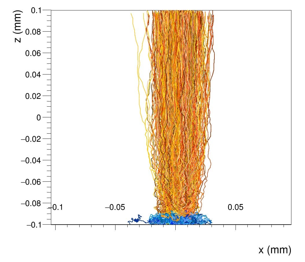
There are several ways now to analyze the situation. To get more clarity, let’s look at what the alpha particle from the Am241 does when hitting your diamond sensor. For this, we add the following configuration to the propagation module:

output_plots = true
output_linegraphs = true
output_plots_step = 100ps

timestep_min = 10ps
timestep_max = 50ps
timestep_start = 10ps
spatial_precision = 1nm

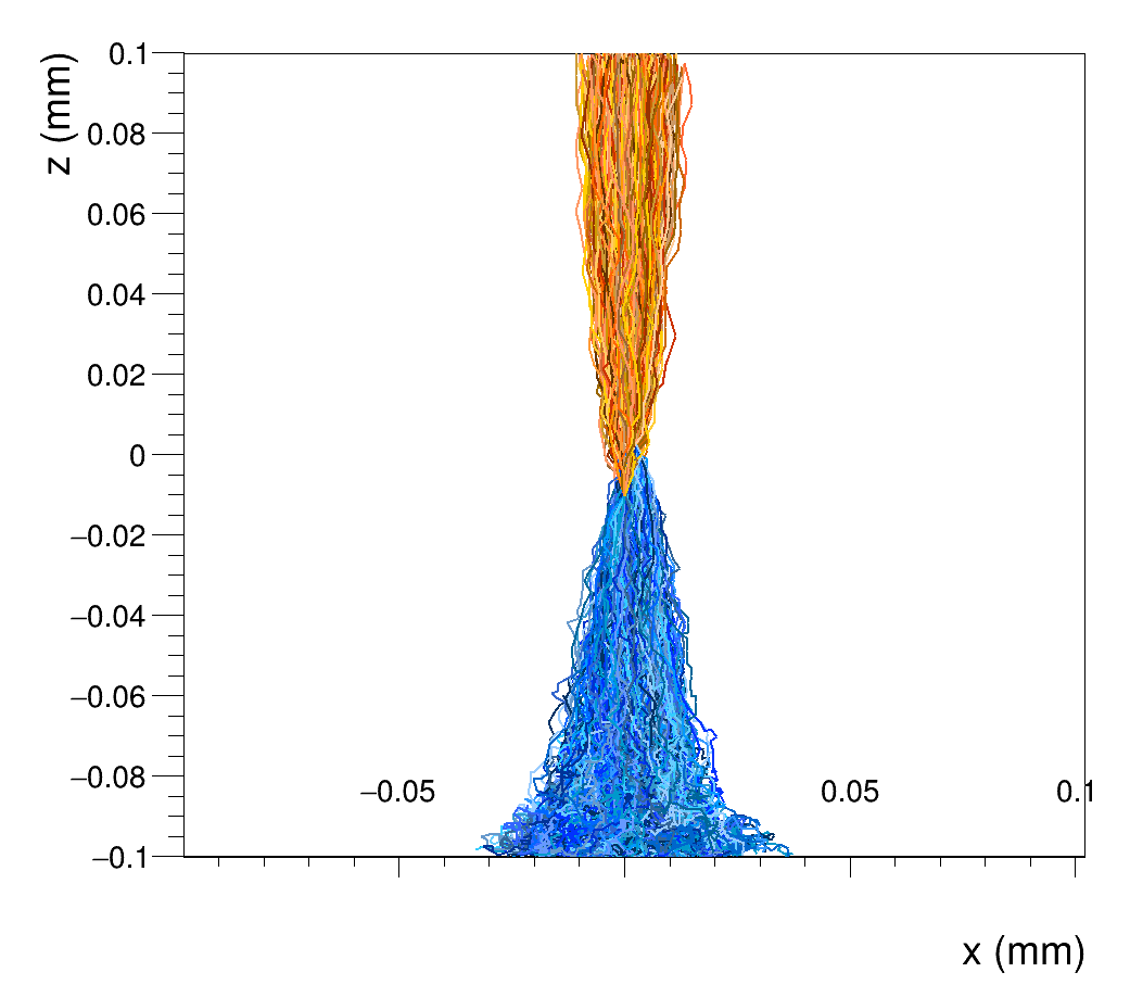
With this, we get line graphs that show the paths of electrons (blue) and holes (orange) in the sensor, drifting along the electric field lines. We can see, that the alphas are mostly absorbed in the center of your sensor:

However, we can also see that towards the bottom of the sensor, the electrons start diffusing strongly. The reason for this is that you have only defined a bias_voltage but no depletion_voltage. We therefore assume the depletion to be the same as your bias_voltage, hence the electric field is zero at the backside (you just barely depleted the sensor).

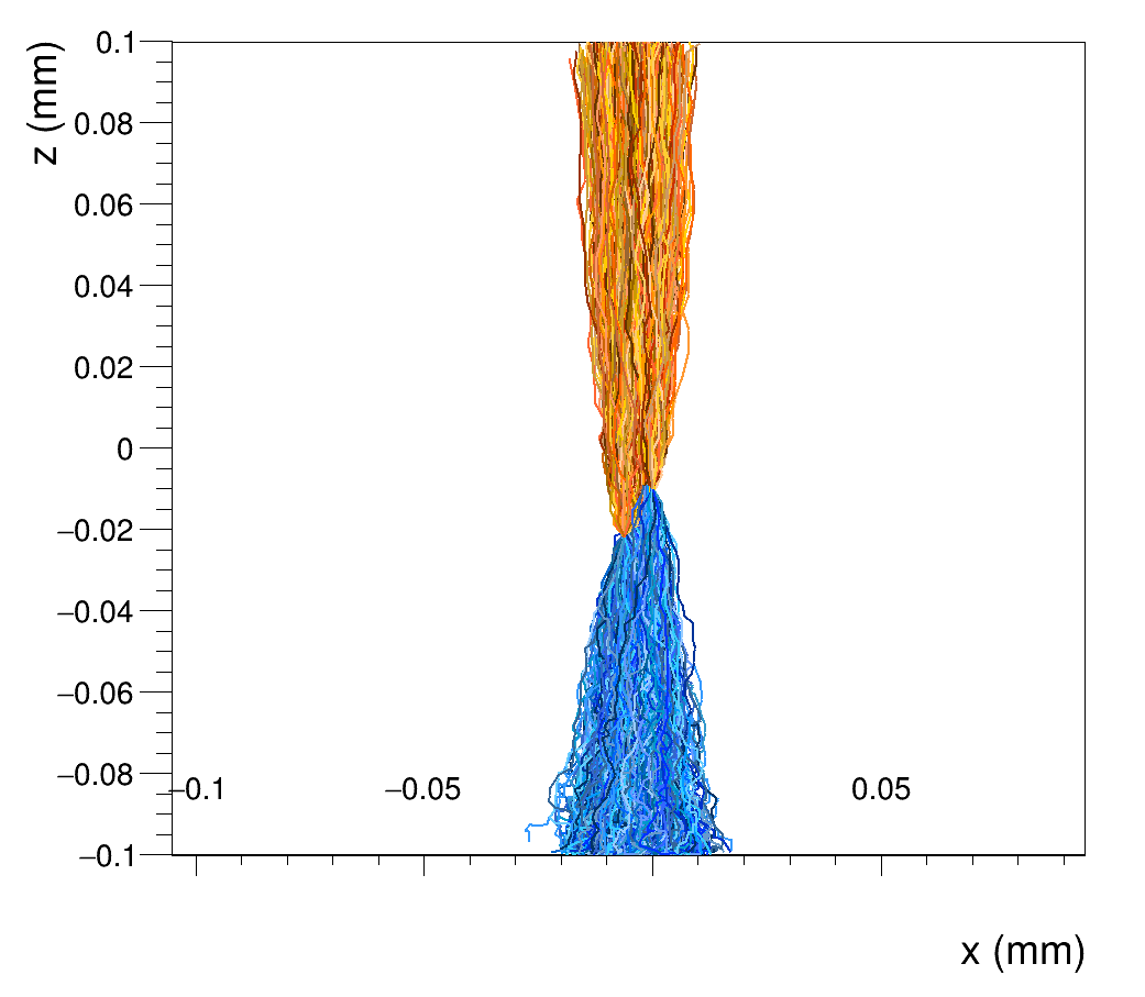
If we overdeplete, e.g. by setting

[ElectricFieldReader]
model = "linear"
bias_voltage = 54V
depletion_voltage = 44V

the picture looks different - we have a stronger field also at the backside and therefore have more drift:

Anyway, back to your configuration with just the depletion voltage provided. We now have two options to look at drift times:

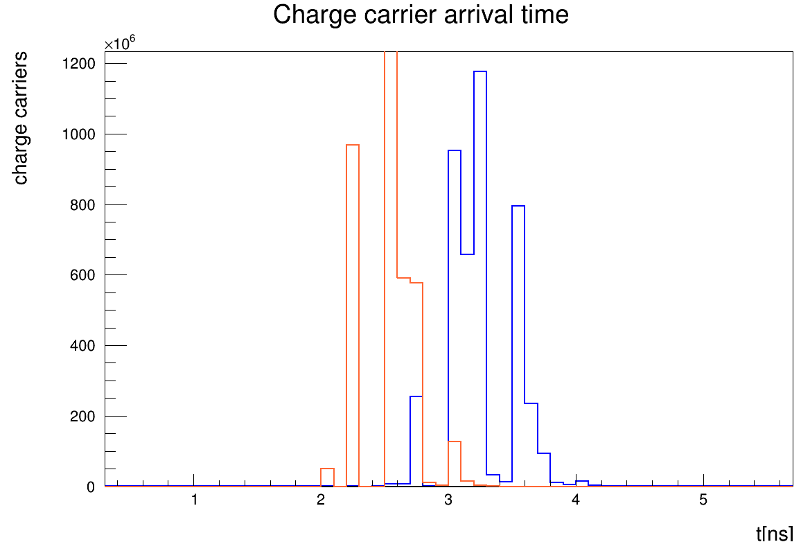
Reversing the bias voltage

In this case you are reversing the polarity of the electric field to collect the other type of charge carriers at the same side of the sensor (front-side). You are only propagating one type of them.

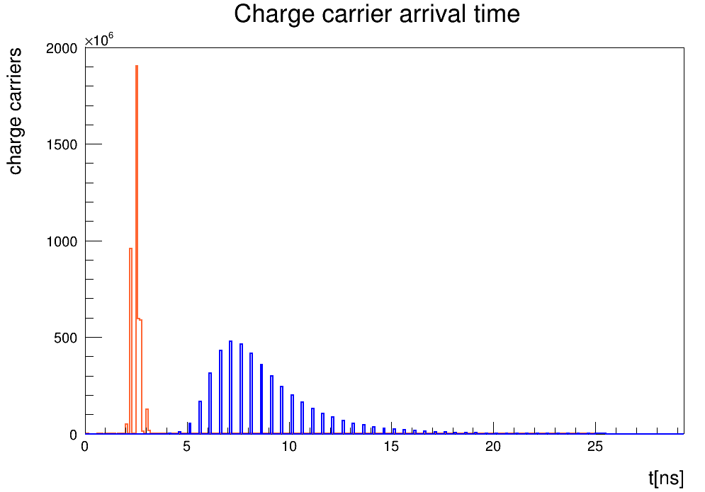
Here you see that the electrons (blue) require (on average) slightly longer to be collected at the front-side of the sensor - which is expected due to their lower mobility in diamond.

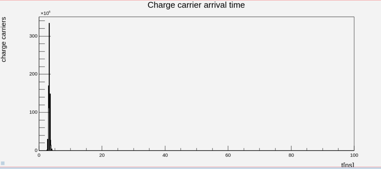
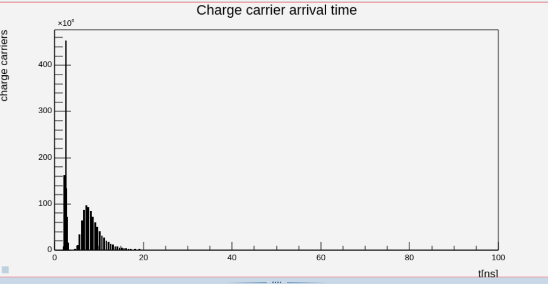
Keeping the bias voltage

If you of course want to know how long the electrons drift to the backside of the sensor, you can propagate them while keeping a positive polarity of your bias voltage. Then you get the longer, smeared-out peak that shows in your second histogram - and by only propagating electrons, we see that it comes from them drifting to the backside:

They take significantly longer than the holes to the front-side because of the very low electric field and the reduced velocity they gain towards the backside of the sensor.

I hope this clarifies the situation and allows you to progress with your simulations.

Cheers,
Simon

Dear @simonspa
thank you very very much for this very nice illustration and guidance. Of course it clarified many things for me and i learned some effective tips for future. Just a short question here.
you mentioned and it is like you mentioned:
We can see, that the alphas are mostly absorbed in the center of your sensor:.
so, my alpha is supposed to be (at least i supposed) somewhere near to the front end electrode, right?
how much can it penetrate the sensor material? it is supposed to penetrate only for few microns (10-15 um) before it is completely absorbed? but here it penetrated 100 microns and absorbed somehow exactly at the center of z-axis. is it the simulation feature that shows the absorbance at center or something is wrong with deposition process? I changed the thickness of sensor from 200um to 400um but still the alpha particle is absorbed at the center of the z-axis. Thank you for your patience.

Hi @sakzai

In your simulation config, you write

 [DepositionGeant4]
 source_position = 0 0 -0.01mm

so your place your Am241 source only 10um away from the center of the global coordinate system. Your detector (in the geometry file) is centered around the global coordinate system, so in this case, your Am241 is built into the detector :slight_smile:

Try moving it out e.g.

 [DepositionGeant4]
 source_position = 0 0 -1mm

Gives me:

Cheers,
Simon

Oh, again thank you very much.