Dear all,
I am observing an unexpected loss in charge collection efficiency (CCE) when simulating an irradiated 100 um thick n-on-p pixel detector.
My goal is to evaluate the CCE as a function of the depth deposition z. So I run several simulations, one per z value using indeed DepositionPointCharge.
I am using v2.3.2.
To run it:
allpix -c main.conf -g detector1.sensor_thickness=100um
It depends on a planar_detector.conf (77 Bytes) and on an electric field and Ramo potential file.
I scan the deposition position in z, by changing in steps of 2 um from -48 to +48 um.
The simulation is done in a 2 Tesla magnetic field oriented as +y.
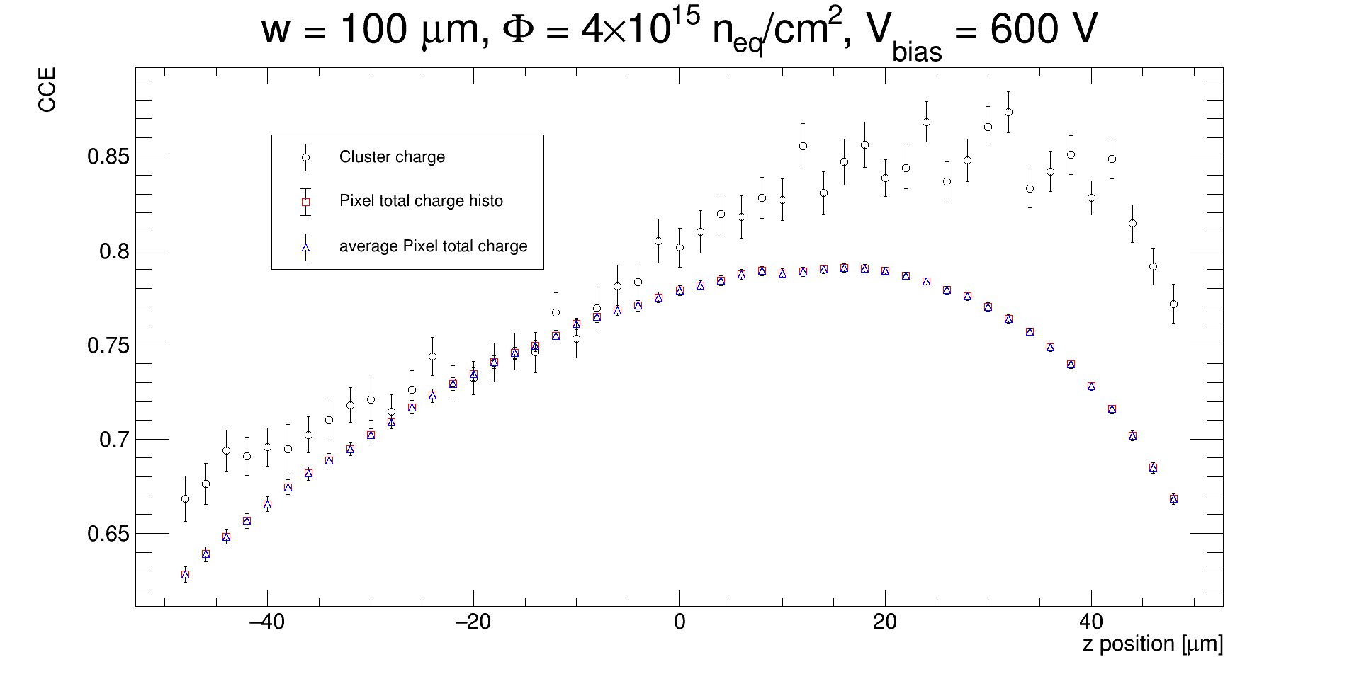
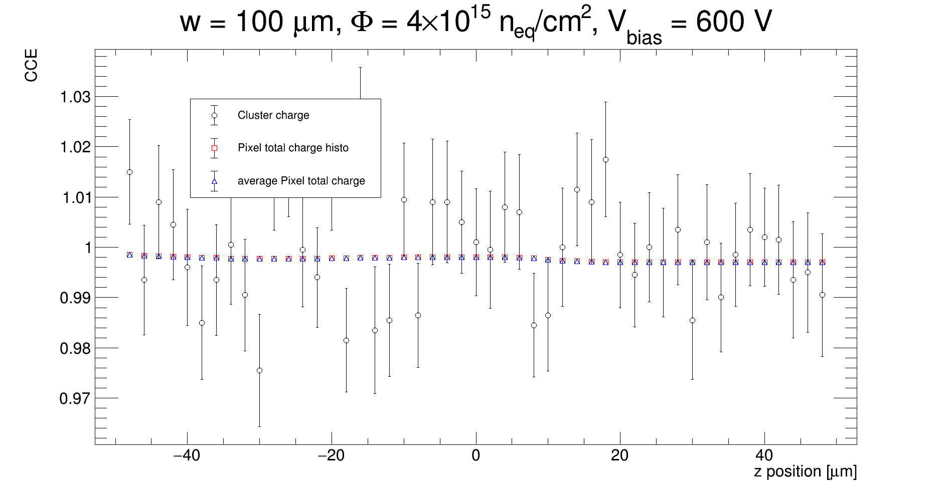
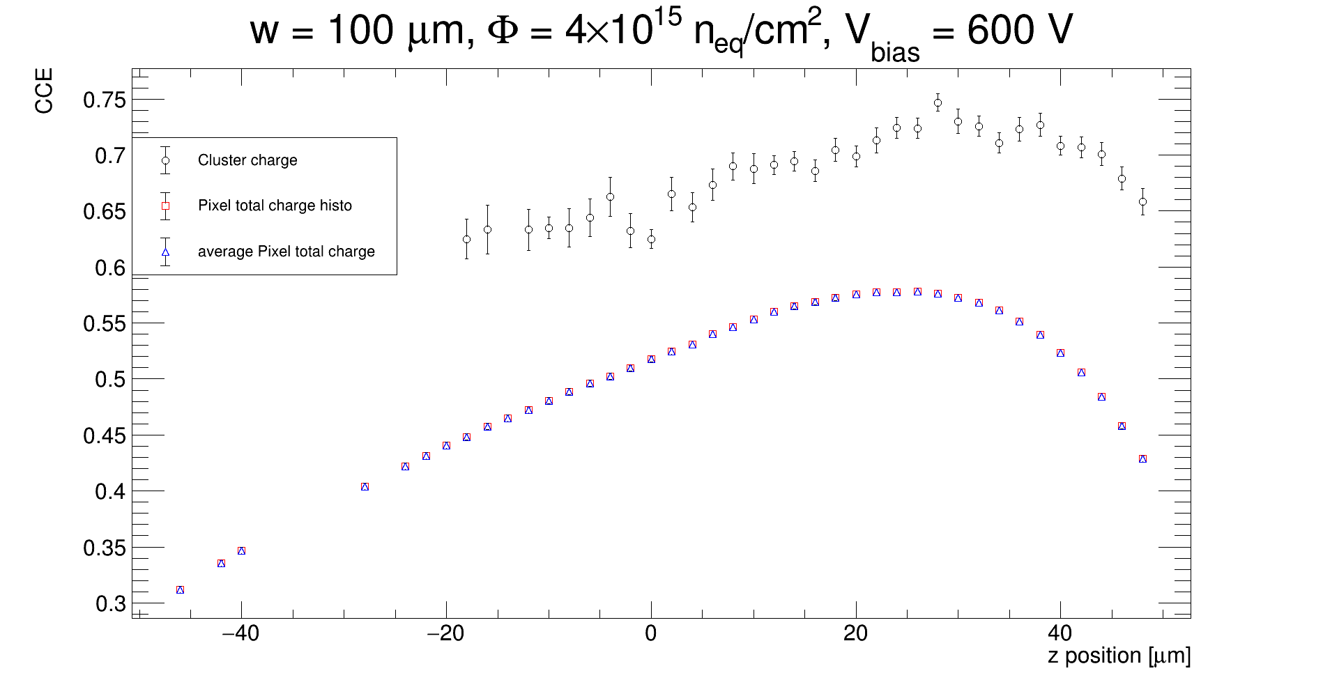
I normalize the charge to the deposited value (1000 e), and I get the following result:
The circles are obtained using the mean value of the cluster_charge histogram in the DetectorHistogrammer folder in the root file.
The squares and triangles are obtained using the PixelTotalCharge variable, using this macro based on one of the examples (the difference between squares and triangles is the following: the former are calculated as the mean of the histogram where all PixelTotalCharges are projected, the latter is done by doing the average not using an histogram; it was a sanity check).
I do not understand the decrease in CCE after z = 20 um, which is very significant when I compare cluster_charge with PixelTotalCharge.
One reason that came into my mind is the coarse (1 um) binning in the implant region but I cannot
convince myself this is responsible for such a large drop in CCE.
So I have two questions:
is there anything wrong in the simulation configuration I am running that explains that drop?
Is there a better (more precise) way to calculate CCE, please?
Any help will be greatly appreciated
Many thanks in advance and best regards,
Marco Bomben and @knakkali
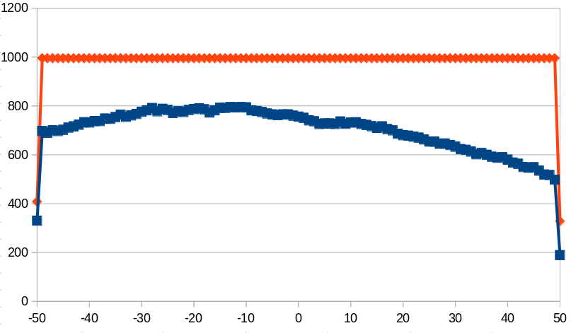
I had a look at your configuration and didn’t see anything odd.
I ran your config, scanning the z position from back- to frontside, juts looking at the total induced charge (sum of all pixels, and without any threshold) - and then I switched off trapping. I get the two curves for 1000e deposited at the respective z position, blue with trapping, orange without. To me it looks like the decrease towards the frontside injection is due to strong trapping of holes on their way to the backside, since without trapping I consistently see 99.5% of the charge induced:
So the presence of a maximum in CCE somewhere in the bulk is confirmed.
At this point I have two questions:
in your reply you mention that you sum the charge of all pixels - would you share the code you used, please?
when using the “ljubljana” several simulations give strange results; indeed I have removed them when I have prepared the plot above, so there are several holes in the graph. You can reproduce some of the problems by setting for example injection z position at -48. I attach the log file of the simulation (209.9 KB) because I don’t see any strange message. Do you understand why this is happening, please?
a few remarks I gathered when looking through your configuration files - some of them might be related to the issues you are describing above, others just tiny observations.
Instead of adding the sensor thickness on the command line with -g you can also place it in the geometry file next to where the position of the detector is defined since you don’t seem to change this for now.
You are storing all objects, especially the DepositedCharge and PropagatedCharge objects themselves are rarely used. In fact, you load the respective trees in your macro, but you don’t actually need them. The total charge (before front-end) induced in a pixel can be retrieved from PixelCharge->getCharge() without looping over the individual connected PropagatedCharge objects. (you do this in pixel_total_charge += pix_charge->getCharge(); already)
I don’t think the calculation of your k_factor is correct. What you are doing right now is to calculate the ration between the total charge of a pixel (from PixelCharge) and an individual deposited charge value (from DepositedCharge, obtained via PropagatedCharge). The latterhas the problem that it is biased in the way you are using it. A propagated charge that does not contribute to your total charge somehow (trapped early on…) would not show up because there is no connection between PixelCharge <-> DepositedCharge. I would instead loop over the DepositedCharge objects separately and sum them so you are sure to catch all initial depositions.
To make this easier we could think of adding the total number of deposited charges as a member of the MCParticle object, I’ll think about that a bit…
You are applying a front-end simulation using a default configuration of the DefaultDigitizer module. Among other settings, this implies a threshold of 600e - make sure to take that into account when analyzing your data, only PixelHit objects with a charge > 600e will be generated!
The log you sent looks fine apart from the fact that all pixels are below threshold - but you are looking at PixelCharge before the front-end anyways.
I personally cheated with my numbers on the total charge, I simply simulated one single event per depth position, and grep’ed the log output for Total charge induced on all pixels: Sorry for being so cheap…
Hello @simonspa
thanks a lot for taking the time to look into this! Your comments are all extremely useful!
Below my comments.
Instead of adding the sensor thickness on the command line with -g you can also place it in the geometry file next to where the position of the detector is defined since you don’t seem to change this for now.
Right, we have could have thought of that
You are storing all objects, especially the DepositedCharge and PropagatedCharge objects themselves are rarely used. In fact, you load the respective trees in your macro, but you don’t actually need them. The total charge (before front-end) induced in a pixel can be retrieved from PixelCharge->getCharge() without looping over the individual connected PropagatedCharge objects. (you do this in pixel_total_charge += pix_charge->getCharge(); already)
ok, so we can use indeed what we call PixelTotalCharge. Thanks!
I don’t think the calculation of your k_factor is correct. What you are doing right now is to calculate the ration between the total charge of a pixel (from PixelCharge) and an individual deposited charge value (from DepositedCharge, obtained via PropagatedCharge). The latterhas the problem that it is biased in the way you are using it. A propagated charge that does not contribute to your total charge somehow (trapped early on…) would not show up because there is no connection between PixelCharge <-> DepositedCharge. I would instead loop over the DepositedCharge objects separately and sum them so you are sure to catch all initial depositions.
That was a first trial when we were thinking of tracking each pixel charge to its own deposited one. When we have discovered it was not possible we decided to run one simulation per depth z so we are sure where the charge was deposited. Indeed now we normalize PixelTotalCharge to 1000, that is the number of electrons we inject.
To make this easier we could think of adding the total number of deposited charges as a member of the MCParticle object, I’ll think about that a bit…
Ok, thanks But it is true that summing over PixelCharge is not too difficult
You are applying a front-end simulation using a default configuration of the DefaultDigitizer module. Among other settings, this implies a threshold of 600e - make sure to take that into account when analyzing your data, only PixelHit objects with a charge > 600e will be generated!
Again, thanks. I could have thought of that
The log you sent looks fine apart from the fact that all pixels are below threshold - but you are looking at PixelCharge before the front-end anyways.
I personally cheated with my numbers on the total charge, I simply simulated one single event per depth position, and grep’ed the log output for Total charge induced on all pixels: Sorry for being so cheap…
That’s very good actually, I can even think of a simpler procedure, although having a tree saved is better
Thanks a lot for all the help, now we understand things at a much deeper level.
Hello all,
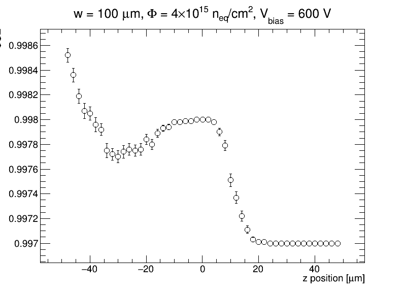
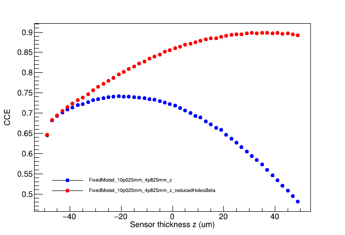
Following the nice and helpful discussion on CCE vs Z in an irradiated detector in the above thread, we tried to do a couple of more studies to understand if the drop in CCE observed towards the pixel side is due to the strong trapping of holes on their way to the backside. In the first test, we reduced the beta values of the holes to reduce the hole-trapping rate. We observed an improvement in CCE to about 42% as you can see in the plot attached below:
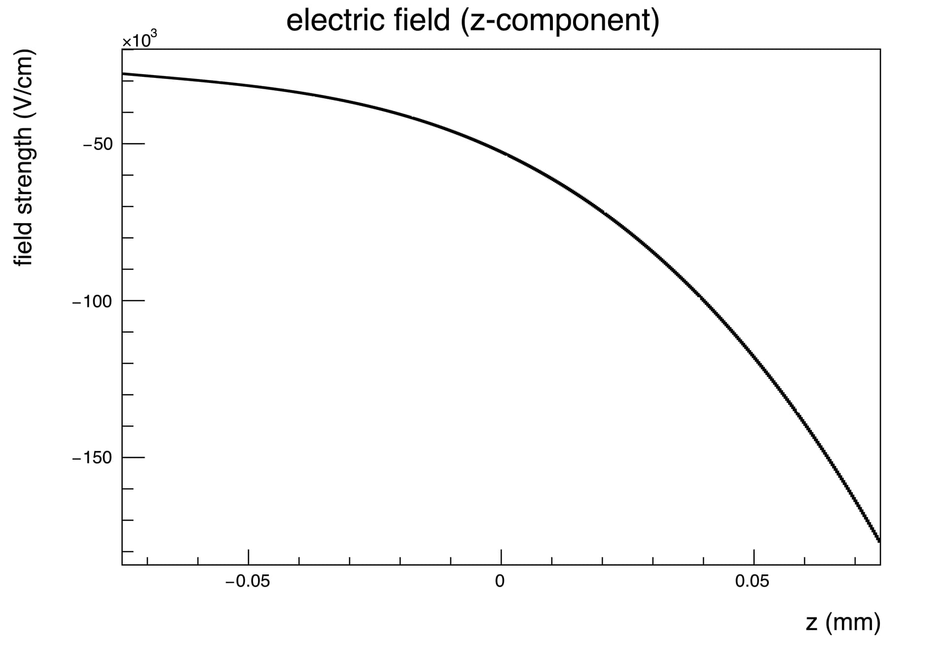
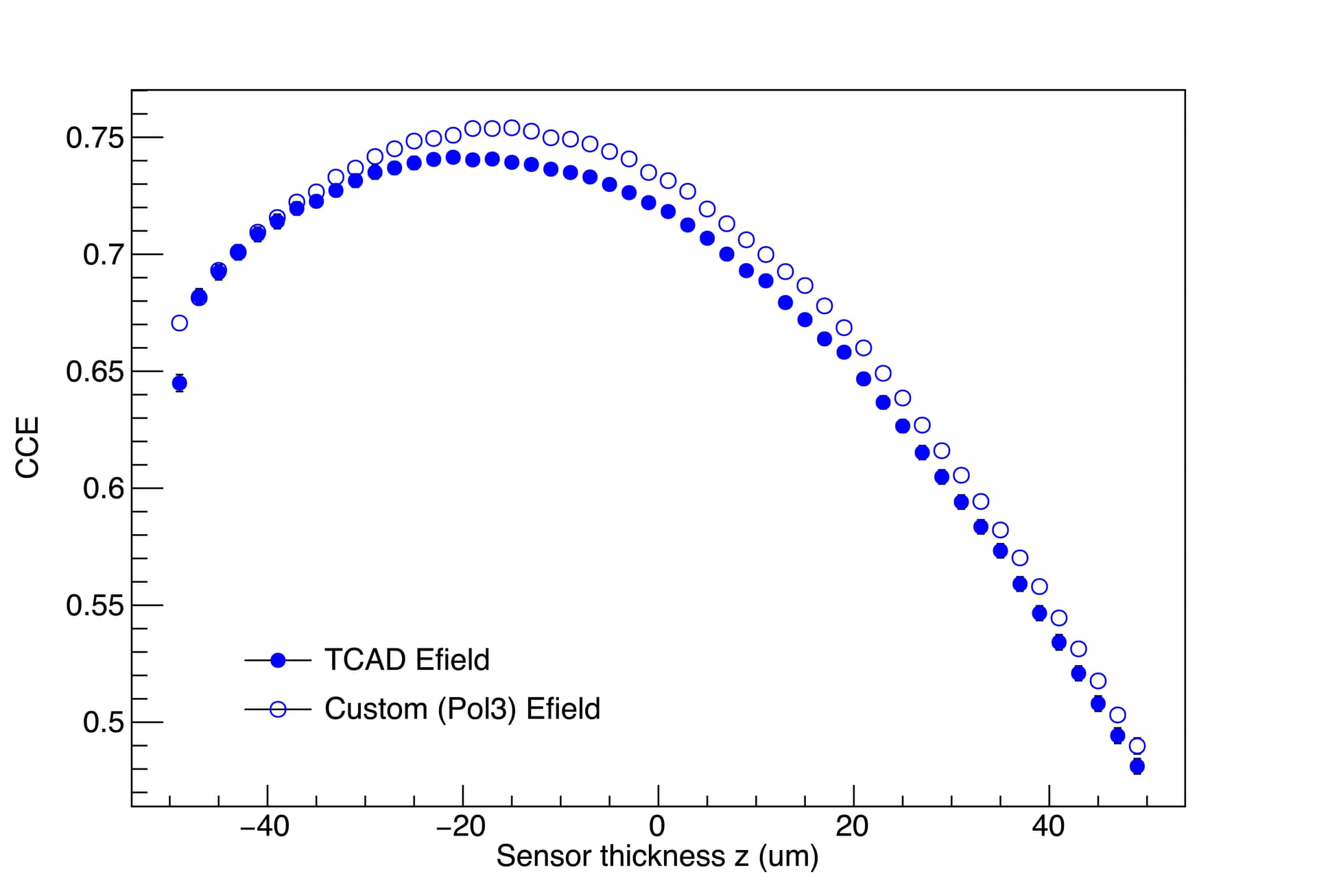
The hypothesis here was that the reduced E-field close to the pixel implants results in lower mobility for the holes created close to pixel implants thereby increasing the probability of holes getting trapped subsequently resulting in lower CCE. To test the effects of low E-field close to the pixel implants, we tried to fit a pol3 to the Z projection of E-field from AP2 using TCAD E-field excluding the low Efield regions and used this pol3 with the fit parameters to use the custom model for [ElectricFieldReader] in AP2. The custom(pol3) E-Field and CCE vs Z using TCAD E-Field and the custom (pol3) E-Field are shown below:
As you can see from the CCE vs Z plot, the effect of low E-field close to the pixel implants seems very small and this is something that we are not able to completely understand.
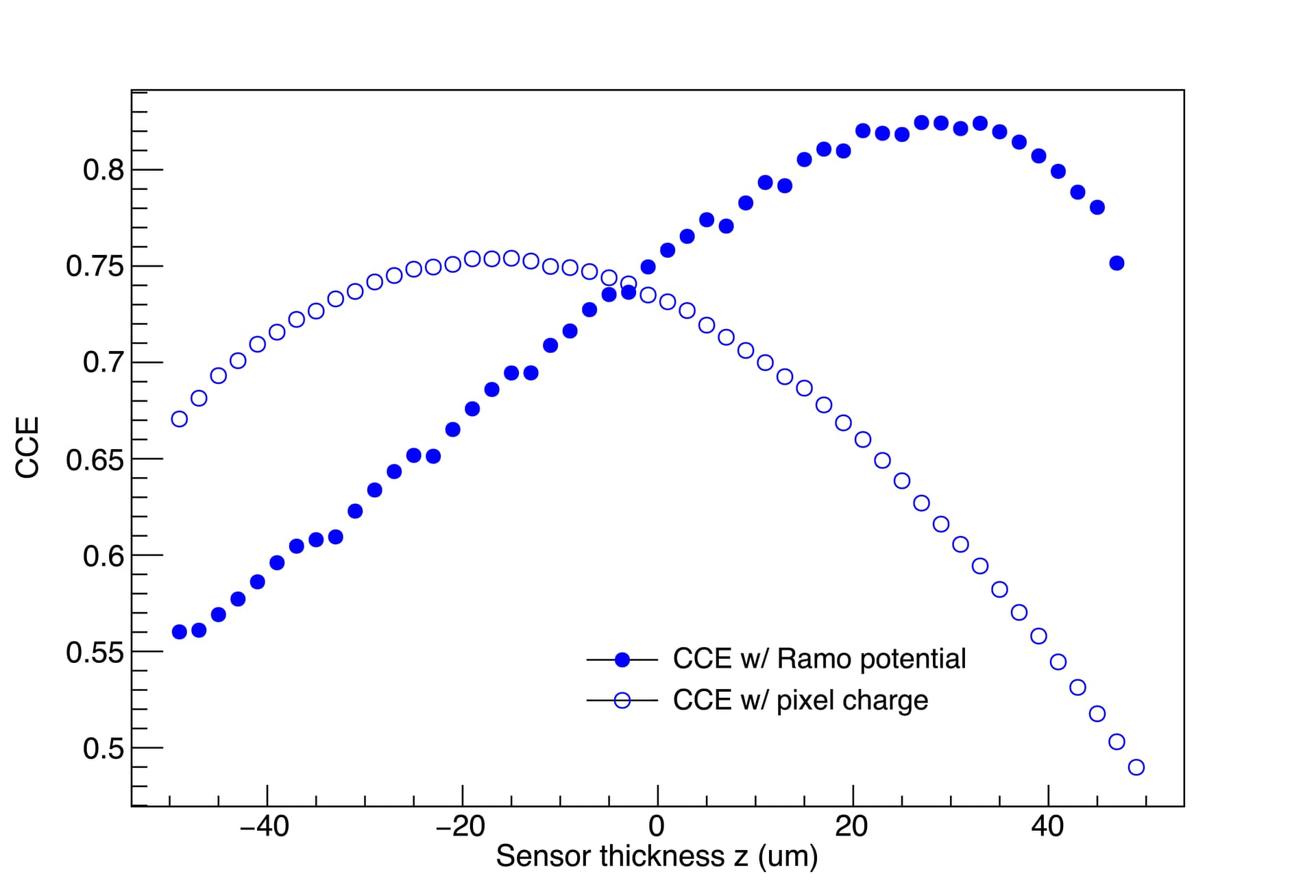
For the next test, we tried to look at the CCE vs Z using the ramp potential. The CCE is here estimated by weighing each bin of PropagatedZ position with the corresponding Ramo potential value. The CCE vs Z distributions computed using Ram potential and using Pixel total charge is attached below:
In principle, we were expecting both distributions to show a similar trend. It’d be great if you can possibly help us understand what we are doing wrong here.
Allpix2 version: 2.3.2
AP2 config for custom E-Field: main.conf (1.4 KB)
AP2 detector file: planar_detector.conf (99 Bytes)
TCAD file: CERNBox
Macro for CCE calculation using Ramo potential: CERNBox
Sorry I was not able to find the edit option to change the plots in my previous post . I’ll post the message once again here. Hopefully all the plots can be seen properly now. Apologies for posting twice.
Hello all,
Following the nice and helpful discussion on CCE vs Z in an irradiated detector in the above thread, we tried to do a couple of more studies to understand if the drop in CCE observed towards the pixel side is due to the strong trapping of holes on their way to the backside. In the first test, we reduced the beta values of the holes to reduce the hole-trapping rate. We observed an improvement in CCE to about 42% as you can see in the plot attached below:
The hypothesis here was that the reduced E-field close to the pixel implants results in lower mobility for the holes created close to pixel implants thereby increasing the probability of holes getting trapped subsequently resulting in lower CCE. To test the effects of low E-field close to the pixel implants, we tried to fit a pol3 to the Z projection of E-field from AP2 using TCAD E-field excluding the low Efield regions and used this pol3 with the fit parameters to use the custom model for [ElectricFieldReader] in AP2. The custom(pol3) E-Field and CCE vs Z using TCAD E-Field and the custom (pol3) E-Field are shown below:
As you can see from the CCE vs Z plot, the effect of low E-field close to the pixel implants seems very small and this is something that we are not able to completely understand.
For the next test, we tried to look at the CCE vs Z using the ramp potential. The CCE is here estimated by weighing each bin of PropagatedZ position with the corresponding Ramo potential value. The CCE vs Z distributions computed using Ram potential and using Pixel total charge is attached below:
In principle, we were expecting both distributions to show a similar trend. It’d be great if you can possibly help us understand what we are doing wrong here.
Excuse me all for my ignorance. Is there any simple automatic way of doing this scan over the z-axis values?
I couldn’t manage to do it or to find the relevant document in the list of documents you provided.
if this is about depositing charges at different depth, you can use the DepositionPointCharge module with its scan function, see documentation here.
If this is about changing the position of your detector, you can change geometry parameters from the command line, just as any other parameter from the configuration, have a look at the relevant section of the manual.
Thanks @simonspa for your quick reply.
I want to scan over the depth, so in z.
He is not using the scan option, yet he was able to scan over z, maybe he used the -g overwriting bash script option you mentioned?
Because with scan option, it will scan over the whole volume of the pixel, I want to scan only over z.
However, I can’t put detector1.position=“0um 0um 15um”, because like this it will move the detector 1, while actually I want to move the deposited point charge along z.
I have been looking into this and I unfortunately don’t have a simple solution for you. I have a couple of questions however:
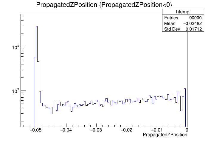
You look at “PropagatedZ” positions - but shouldn’t they all be at top or bottom surface after you finished propagation? Is there a non-zero distribution of those on the central sensor region?
I can’t follow your argument with “weighting with Ramo potential” - the induction happens through potential differences, so only when you have a movement, the induced current corresponds to the charge times the difference in weighting potential before and after the step.
You look at “PropagatedZ” positions - but shouldn’t they all be at top or bottom surface after you finished propagation? Is there a non-zero distribution of those on the central sensor region?
Why should they? They are trapped at different positions according to trapping time distribution.
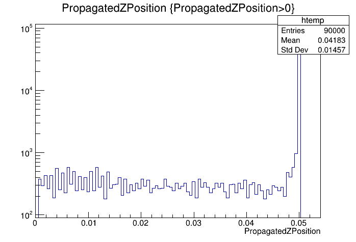
Please see below for injection in the mid-plane the final position of electrons:
As you can see both electrons and holes are “spread” along the bulk; the average value of the histograms gives an idea already on how much electrons travel more than holes.
I can’t follow your argument with “weighting with Ramo potential” - the induction happens through potential differences, so only when you have a movement, the induced current corresponds to the charge times the difference in weighting potential before and after the step.
We are looking at integrated signal to estimate CCE so our reasoning is the following: as the initial position is the same for electrons and holes we can just look at their final positions.
Suppose you have just one electron-hole pair, produced at z_inj and let f be the weighting potential.
Then, if z_e (z_h) is the final position - i.e. propagated_charge->getLocalPosition().Z() - reached by the electron (hole), your induced signal q will be:
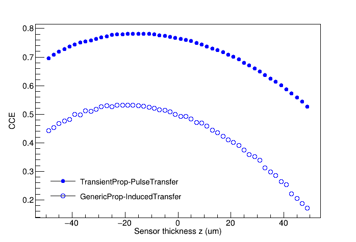
I had a chat with @pschutze about the discussion you had with him, and I think I now have a better understanding of the situation.
If I understood correctly your cross-check should be very similar to running GenericPropagation and afterwards InducedTransfer (see documentation here) which essentially takes initial and final point for all charge carriers and calculates the total induced current.
Maybe that setup is simpler because you’re not simulating the full transient behavior.
Thank you so much for your reply. One of @pschutze 's suggestion during our chat last was indeed to use [GenericPropagation] instead of [TransientPropagation]. We tried running AP2 simulations with 3 different configurations:
Test #1: [TransientPropagation] followed by [PulseTransfer]
Test #2: [GenericPropagation] followed by [InducedTransfer]
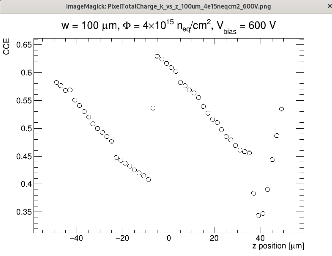
Test #3: [TransientPropagation] followed by [InducedTransfer]
The CCE vs Z distributions we have in the above 3 cases are attached below:
The plot on the left is the comparison of CCE vs Z when we use [TransientPropagtion] followed by [PulseTransfer] and [GenericPropagtion] followed by [InducedTransfer]. When we use the latter config, the CCE is low by ~0.2% at every Z deposition position.
The plot on right corresponds to test #3 ([TransientPropagation] followed by [InducedTransfer]). We understand that [InducedTransfer] is a module for non-time resolved simulations performed with [GenericPropagation]. We wanted to check and see the results when used in combination with [TransientPropagation]. Our expectation was that the distribution would be similar to what we obtained earlier when we estimated CCE by weighing each bin of PropagatedZ position with the corresponding Ramo potential value. However, based on what we can see in the graph, it appears that using [InducedTransfer] in combination with [TransientPropagation] may not yield desirable outcomes…