I am trying to make some simulations for a monolithic pixel sensor.
The idea is that I am using the DepositionPointCharge module and deposit charge carriers in different areas of the pixel and see the percentage of charge going for each pixel (seed or neighbor or …).
I put 100 events in the [Allpix] module and 100k charge carriers in the [DepositionPointCharge] module: --------------------------------------------------- [DepositionPointCharge]
*** log_level = DEBUG***
*** source_type = “point”***
*** model = “fixed”***
*** position = 0um 0um 0um***
*** number_of_charges = 100000*** --------------------------------------------------
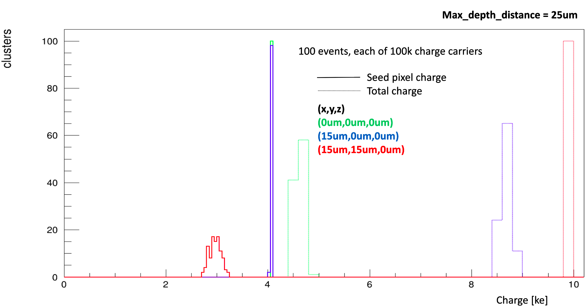
I chose as a start three places to deposit, (0um,0um,0um), (15um,0um,0um) and (15um,15um,0um).
That are respectively “pixel center”, “pixel side” and “pixel corner”. (The terminology may not be accurate but the main idea should be understood from the coordinate values assuming a square pixel of 30um pitch).
The problem I am facing is that when I see the plots in the DetectorHistogrammer: seed_charge and total_charge: First, I expect that the total_charge should be constant for the three cases regardless of the deposition position, which I don’t see in the plots, every case has different mean of total_charge. (see the file attached) Second, When I deposit 100k charge carriers, I expect to have total_charge in the order of 100k (or 50k if half are holes and half are electrons), which is not true at all in the results, I am having a histogram of a mean around 10k e. Since recombination and trapping are both none by default, so there is no other source of loosing the charge that we deposit.
I tried to play with the parameter max_depth_distance in the [SimpleTransfer] module to collect charge from all the pixel and went from 3um to 25um to 50 um which is the whole thickness and still the same issue.
Please if you can point out what I am misunderstanding.
there are a number of places where things could go wrong, many just mere configuration issues. Would you mind attaching your used configuration files? I can then check for the ones that came to my mind and let you know where to continue looking.
@simonspa Thank you for your reply!
Here is the file, it was used to generate the green plots, the others are just a copy with different deposition position. main_pos1.conf (1.4 KB)
The geometry is just a monolithic pixel sensor, ALPIDE like.
And please If you can help me with understanding somethings in the config file, that may be related to this issue:
1- How important is the depletion_depth parameter if we anyway import the E field from TCAD? It is not mandatory but does eliminating it affect the simulation accuracy? I tried removing it and compared the E field shapes and found totally the same structure for the ElectricFieldReader histograms.
2- I suspected that the integration time may have an effect in not collecting everything, as it is 25ns here. But we are collecting charge from all the pixel, so it shouldn’t affect, right?
3- I am confused between collect_from_implant (Note: it is commented in the config file I attached, but wasn’t commented in the simulation I did to get the results I showed) and the max_depth_distance parameter, for the SimpleTransfer module. If I use both, won’t it be a contradiction, asking the software to collect charges from implants and also at the same time to collect it from all the pixel with depth 25um?
4- When I converted the TCAD files, I put one time as a try: xyz = xyz, and one time xyx = xyz, both cases gave the expected E field shapes in the ElectricFieldReader. So how possible? I did this because I don’t know the coordinate system of the TCAD files I got from my colleague, and he is not sure because he somehow mixed between old and new versions of TCAD.
With the depletion_depth you can stretch or shrink the field along the depth. For example, when simulating CMOS sensors (like you do, judging from the mimosis model name) TCAD simulations often only cover the top epi layer while the thick substrate is not simulated. With the depletion_depth parameter youc an assign the field e.g. to the top 10um while the rest stays undepleted and carriers will diffuse there.
Yes the integration time can have a strong impact on which charge carriers make it, especially when looking at low-field CMOS sensors that might include significant diffusion. Make sure to also look at other histograms that are e.g. provided by the propagation module to help you figure out if this is the case.
Are we collecting from the whole sensor though? You set max_depth_distance = 25um but your sensor is 50um thick according to your previous statement.
In v2.3.x the implant is a 2D area defined on the surface of the pixel. Switching it in or off will mean either taking carriers from the full surface of the pixel, or just from the region defined by the implant. If you did not define implant_size in your model (which I cannot check without that file…) it will by default cover the full pixel.
The max_depth_distance in addition governs how deep we look from the surface down into the sensor. This is relevant when you have e.g. high-dose implants as collection electrodes that have zero field within them but that have a depth of a few micron. In the zero field region, the carriers don’t move to the surface anymore, so you need to make sure to collect them also from a depth of those few micron.
I assume you don;t actually mean xyz = xyz in both cases If you flip x and y your field might just be rotated by 90deg around the z axis.
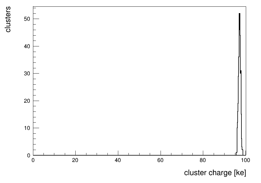
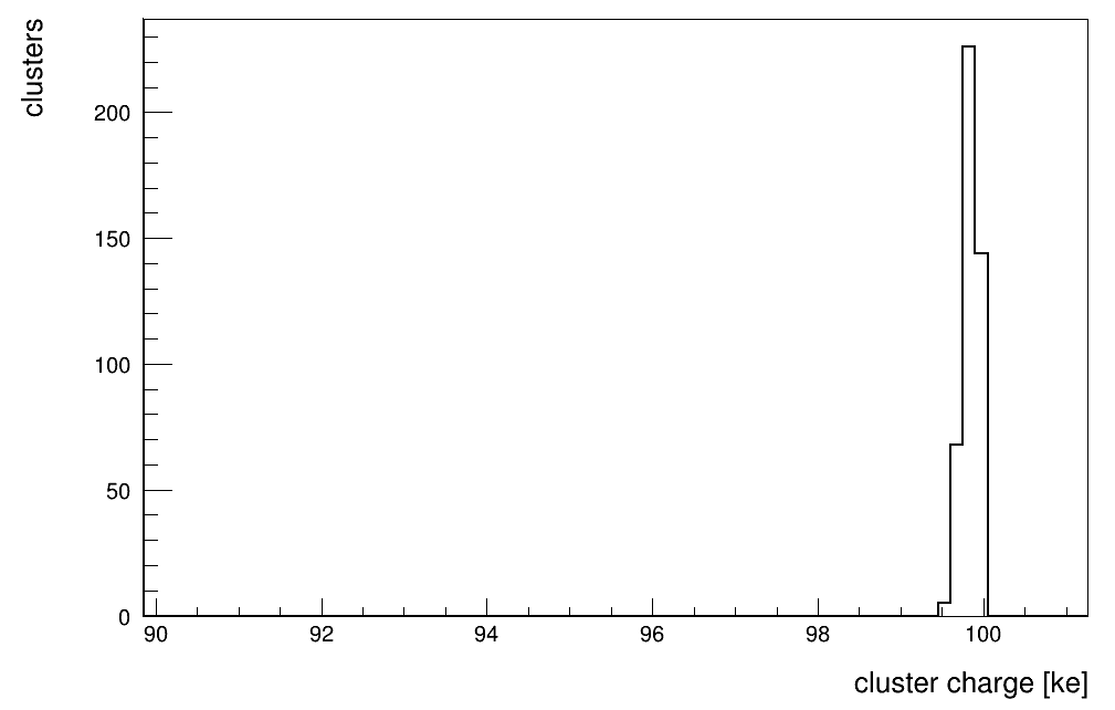
…slight offset towards lower values comes from the fact that you’re in the lower-left pixel and some charges hit the sensor wall. Moving it to the next pixel (adding once the pitch to x and y) gives you a nice peak at 100k with slight smearing to lower values coming from threshold effect when sharing charge: