Hi~!
Sorry for the sudden question. I have a few questions that confuse me:
In pixel model building, if I want a pixel with a substrate thickness of 200um and an epitaxial layer of 45um thickness, what parameters should I use?
From the user manual, I speculated that the thickness of the pixel epitaxial layer should be represented by sensor_thickness = 45um. But the substrate thickness is chip_thickness=200um?? * In fact, I think my understanding is flawed…
2.In the geometric construction of pixels, I can only define the material of the epitaxial layer as Si. Is there a way to set the doping concentration? I personally believe that doping concentration may affect carrier diffusion and lifetime.
In the process of importing the electric field from the TCAD, I was thinking that the process we used in Allpix^2 to fill the entire pixel array by copying a single electric field, did we consider the problem that the edges of the electric field between the pixels may not be connected?
Do we have a way to test this problem? For example, look at the electric field distribution of the overall pixel array, etc…
Maybe my question is a bit superficial, but I couldn’t find an accurate description to solve my confusion. Looking forward to the developers’ replies!
What you need to do is to define the sensor_thickness = 245um. The manual claims the following for monolithic sensors (I assume this is the case), where the last sentence answers your question:
The base parameters described above are the only set of parameters supported by the monolithic model. For this model, the chip_thickness parameter represents the first few micrometers of silicon which contain the chip circuitry and are shielded from the bias voltage and thus do not contribute to the signal formation.
For this, there’s a dedicated module, the DopingProfileReader. You can either load files converted from TCAD simulations, or define regions in depth with certain concentrations. Please find the corresponding section in the manual here: https://project-allpix-squared.web.cern.ch/project-allpix-squared/usermanual/allpix-manualch8.html#x9-1690008.11
This creates information on local doping concentrations and influences mobility and lifetime, if the corresponding models are selected in the propagation.
Thanks for your reply! I still have some questions that I feel are a little tricky.
I’m curious about how do we divide the substrate and epitaxial layer of the pixel? Is it divided according to the electric field of the TCDA we imported? Or do you need to introduce the doping concentration of the substrate and epitaxial layer? Or something else I don’t know at the moment.
Sorry to bother again, look forward to hearing from you again.
In the detector model not at all, there you just provide one slab of silicon (just as when you handle it in the lab). The two only differ by the doping concentration, so see answer below.
Here it depends a bit. If your TCAD simulation only comprises the epitaxial layer but you have not simulated the substrate, then you can do
This will map the imported electric field to the top 45um of the sensor and leave the rest of the sensor undepleted.
Also here it depends. If you have a doping concentration you would like to import from TCAD, you can do a similar trick as for the electric field above using doping_depth. There is one difference: the DopingProfileReader will take the last doping value found (so the last bin in your simulation along depth) and use this as the doping concentration for the rest of the sensor. Also this is described in the user manual.
Alternatively, and maybe enough for your purposes, you can set regions of doping using
[DopingprofileReader]
model = "regions"
doping_concentration = [[20um, 100000000000], [100um, -3000000000000]]
where the two values are depths and concentrations for the sensor up to the given depth. The sign encodes the dopant type.
Thank you for your reply!
I’m sorry to be so abrupt again. When I imported the field file of TCAD, everything worked fine.
However, when I imported the electrostatic potential distribution of TCAD, it showed abnormal, which made me very confused.
|17:16:29.109| (WARNING) [I:WeightingPotentialReader:Dedx_Epi5] No field units provided, interpreting field data in internal units, this might lead to unexpected results.
|17:16:29.110| (ERROR) [I:WeightingPotentialReader:Dedx_Epi5] Requesting to interpret INIT field as units “” while file header states “V”
|17:16:29.118| (FATAL) [I:WeightingPotentialReader:Dedx_Epi5] Error in the configuration:
Value “./TCADFile/T1_Epi1_xyz_ElectrostaticPotential.init” of key ‘file_name’ in section ‘WeightingPotentialReader’ is not valid: Unphysical weighting potential detected, found -1.951400 < phi < 0.448496, expected 0 < phi < 1
The configuration needs to be updated. Cannot continue.
My electrostatic potential file ElectrostaticPotential.init looks pretty good. Would you mind telling me what caused the problem?
you are trying to load an electric potential as weighting potential, but these are two different things. Please have a look at Field Maps | Allpix Squared
You need to have two electric potential maps with slightly different voltage on the collection electrode, and then subtract and normalize them.
If I understand correctly, the WeightingPotentialReader module is mainly used to describe the case that the electric field imported from TCAD is not a complete pixel cell.
In addition,
when I exported the electric field file imported from TCAD into the electrostatic potential related file, I used it in [ElectricFieldReader], but the result was still disappointing. Is it because the [ElectricFieldReader] module can only handle the vector form of ElectricField, but not the scalar form?
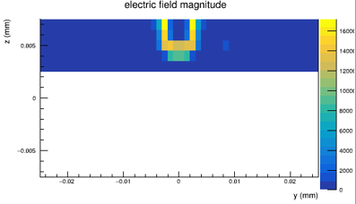
I wanted to use the electrostatic potential to see the rationality of my electric field distribution, but unfortunately I didn’t find a reasonable way to visualize the electrostatic potential distribution. Just from the electric field distribution(see Fig1
), I don’t know what the physical meaning of its numerical value is.
[The xy axis is the position, so what’s the physical meaning of the number on the right]
If I understand correctly, the WeightingPotentialReader module is mainly used to describe the case that the electric field imported from TCAD is not a complete pixel cell.
Sorry to say it that bluntly, but you do not understand correctly:
The Electric Field is the vector field governing the drift of charge carriers. We need a vector field here because the drift is a directional movement.
The Weighting potential is a potential and therefore a scalar field. It is used in the context of the ShockleyRamo theorem to calculate induced currents. It needs to be normalized to unit potential.
So what you are experiencing should not be disappointing, but it is physics. I would really urgen you to read the respective sections in the user manual.
I wanted to use the electrostatic potential to see the rationality of my electric field distribution
I am not sure what you mean by “rationality” in this context, but the units of the colored z axis will be visible if you rescale the histogram a bit on the right. It is V/cm.
After your explanation, I think I need to read the relevant chapters of the user manual carefully. My question is really a little superficial.
In fact, I have another questions about electric field distribution:
As we all know, due to the difference in doping concentration between substrate and epitaxial layer in CMOS sensor, a certain barrier electric field distribution will be formed between them. If I only import the electric field distribution of the epitaxial layer, will it affect the actual simulation results?
(In my mind, the barrier electric field distribution between the substrate and the epitaxial layer will cause the carrier to move in the epitaxial region, if not, I can not anticipate the carrier movement at this boundary.)
In addition, how do particles move around the edge of the pixel array? Will the particles be absorbed or reflected, or both.
You should model the transition region in your TCAD simulation. Then the respective field forms properly and is taken into account for propagation.
If you mean “particles” as in “beam particles” they will just continue tracking. If you are talking about charge carriers (“quasi-particles”) then they are absorbed at the edge since we assume a dicing edge that will introduce many defects.
I have some confused. Would you mind telling me where the source code of relevant Settings is it?
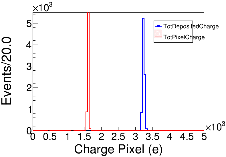
Q2: Under your guidance, I carried out a simple simulation. I wanted to see the distribution of total deposited charge and total pixel charge distribution under each Event, and I got the distribution as shown in the figure c1.1. My incident particle is a Gamma of 5.9keV. Why am I able to get about 3.3ke of electrons? (I guess this is recording both electrons and holes, but how do I tell them apart?)
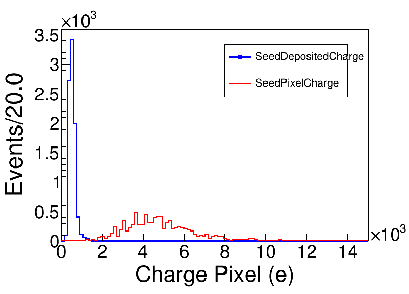
Q3: I want to analyze the seed pixel charge and its corresponding MCTruth charge. Therefore, using method:
     int DeC = 0;
      if(w1_Seed_hit != nullptr){
      std::vector<const allpix::PropagatedCharge*> Propagated_Charges = w1_Seed_hit->getPixelCharge()->getPropagatedCharges();
         for(auto&ProCharge : Propagated_Charges){
             //output_seed_DepositedCharge.push_back(ProCharge->getDepositedCharge()->getCharge());
             DeC += ProCharge->getDepositedCharge()->getCharge();
          }
          output_seed_DepositedCharge = DeC;
       }
, I obtained its corresponding distribution, but the charge distribution of Truth was much higher than the quantity of 3.3ke, which I could not understand.
Not sure what you mean. Electrons and holes are absorbed e.g. here
Yes, you are double-counting because they are stored separately. Use DepositedCharge::getType() to check which one it is, see here
As said above, you’re double-counting charge carriers. The pixel charge is the correct value, since there you’re only looking at the charges arriving at your electrode (or induced current, depending on the used propagation module)
I can’t tell more because I neither have the rest of your analysis code nor your simulation config.
Hi~Thanks for your help.
The simulation I want to do so far is by adding a reverse bias so that our electrons are collected from N-well.
Can I do this with “implants”? Or do we need some other parameter settings? Is the setting of the implant this parameter “implant_size”?
Hi! I’m sorry to interrupt.
I wonder if I could ask you how to use mesh_converter to get the Weighting potential file required in the WeightingPotentialReader module, as I don’t know how to write that configuration file?
I looked at the user manual, and it didn’t tell me exactly how to write the configuration file to get the weighted potential, right.
Generating a weighting potential using TCAD and Allpix Squared
The weighting potential is calculated by taking the difference of the electrostatic potentials arising from applying two slightly different bias voltages to one electrode.
The steps below outline how to create a weighting potential from TCAD simulations.
Produce two TCAD fields that differ slightly in one collection electrode bias voltage, for instance for 0.1 V or 0.01 V, with all the other electrodes grounded. Export the DF-ISE .dat and .grd files containing the electrostatic potential.
Use the mesh_converter tool to extract the electrostatic potential from both configurations. Working with the converted files in INIT format is advisable as is human readable and this makes the process of writing a macro for the calculation simpler.
Calculate the difference between entries from both files, and divide them by the difference in collection electrode bias voltage.
Verify that the values are within a range from 0 to 1, which is the physical range of a weighting potential.
Save the resulting file with the same format and import it into Allpix Squared using the [WeightingPotentialReader] module and the mesh model.
Sorry to bother you again, but I still have a few questions that are confusing me.
If I only import the electric field distribution and doping concentration distribution from TCAD, but do not import the weighted potential, will this affect my charge collection efficiency? Empirically, the charge collection efficiency of the chip I’m trying to simulate should be around 90%, but my simulation results are only 30%.I’m trying to figure out which of my steps might have gone wrong.
you only need the weighting potential when you would like to look at time-resolved simulations (using TransientPropagation). Otherwise it is not necessary. Depending on your detector, the simplified charge transport models should not affect your CCE.