Hello AllPixers,
I am currently a beginner of Allpix^2 software and I am having a little trouble with the result analysis after importing the TCAD electric field file. Looking forward to your reply!
I am trying to make some simulations for a monolithic pixel sensor.
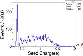
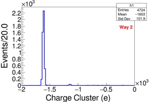
When I select an ordinary linear electric field with a bias voltage of -1.5V, the depletion layer depth is 5um. In the obtained seed pixel charge distribution, there is a relatively obvious peak in 1.6ke[See Fig.1]. (The average energy required to produce an electron hole pair at room temperature is 3.6eV, and the logarithm of the electron hole produced by a 5.9keV photon in silicon is about 1639.) And the distribution of charge collected by the cluster is Fig2;
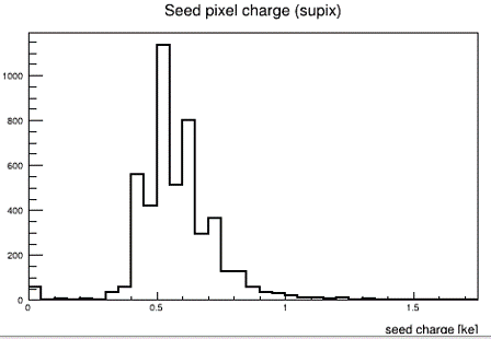
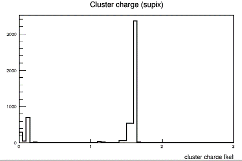
However, when I imported the electric field file simulated by TCAD, I found that the charge quantity of its seed pixel did not peak at 1.6ke (See Fig3). By the way, from the distribution of charge collected by the cluster, a small number of gammas are not fully absorbed (See Fig4).
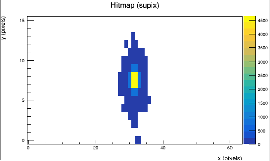
- However, from the perspective of the distribution of hit pixels (See Fig5), the distribution of the low end of cluster may be caused by the incident particles hitting the edge of the array is not completely deposited. Right?
- Is it a problem with the input field I imported from TCAD that makes my seed pixel distribution so poor? (In my expectation, some particles should be completely deposited in a pixel, making the seed pixel have a peak around 1.6keV, even if the peak is small)
3.By the way, I think there is a problem with parameter setting? I don’t really understand the meaning of the following parameters:
sensor_thickness [Parameters that appear in the define models]
chip_thickness [Parameters that appear in the define models]
depletion_depth [Parameters that appear in [ElectricFieldReader] ]
- Or should I add some other variables to my simulation file?
This problem has puzzled me for a long time, but I still can’t find the reason why my seed pixel distribution does not meet expectations. The above four analyses are a guess of mine, and I am not sure whether it is reasonable.
My geometry model is as follows:
type = “monolithic”
geometry = “pixel”
number_of_pixels = 64 16
pixel_size = 21um 21um
sensor_thickness = 18um#chip_thickness = 30um
#sensor_material = “Silicon”
[support]
thickness = 30um
size = 2mm 7.88mm
location = “sensor”
material = “g10”
My simulation file is as follows:
[AllPix]
log_level = “WARNING”
log_format = “DEFAULT”
number_of_events = 10000
detectors_file = “Supix_geometry.conf”
model_paths =“custom.conf”[GeometryBuilderGeant4]
world_material = “air”[DepositionGeant4]
record_all_tracks = true
physics_list = FTFP_BERT_LIV
particle_type = “gamma”
source_energy = 5900eV
source_position = 0um 0um 3mm
source_type = “beam”
beam_size = 1um
beam_direction = 0 0 -1
number_of_particles = 1
max_step_length = 1.0um
output_plots = true[ElectricFieldReader]
model = “mesh”
file_name = “elecFile_supix1_ElectricField_SiEpi_100W.init”
output_plots = true[GenericPropagation]
temperature = 293K
charge_per_step = 100
integration_time = 32us
propagate_electrons = true
propagate_holes = false[SimpleTransfer]
max_depth_distance = 18um
output_plots = true
output_plots_step = 0.1ns[DetectorHistogrammer]
name=“custom”[ROOTObjectWriter]
file_name = “test.root”