Reasons for low Charge collection efficiency

Hello,
sorry to interrupt, I think I have some new problems. Through some experience on the forums, I tried to solve these situations myself, but unfortunately, I spent a lot of time and still had a hard time solving them.

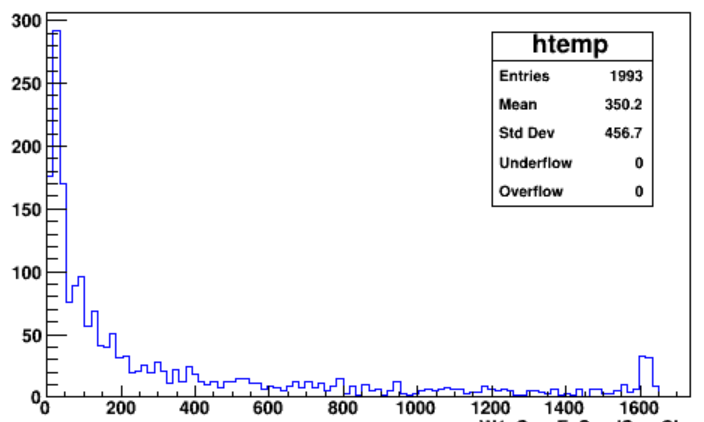
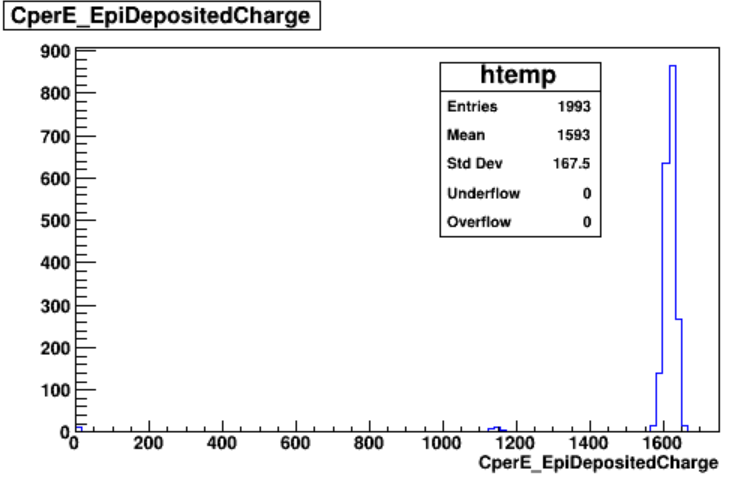
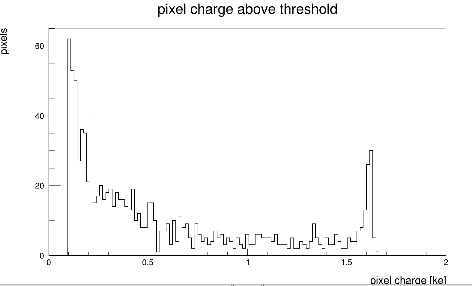
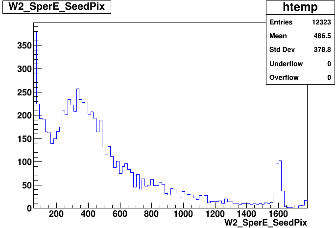
I am currently simulating a high-resistivity epitaxial layer, and theoretically, some of the currently known experimental processes have a charge collection efficiency close to about 100% for their measured clusters, such as ALPIDE. So when I got only 30% of the results, I was confused.

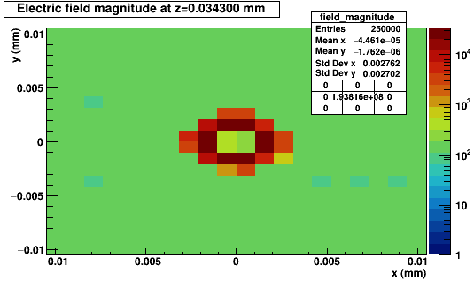
After analyzing the recorded deposition energy and considering the energy that generated the electron-hole pair, I felt that the charge deposition part of my simulation was fine.

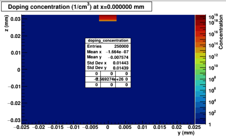
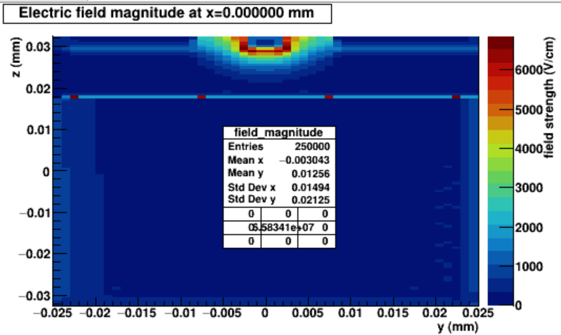
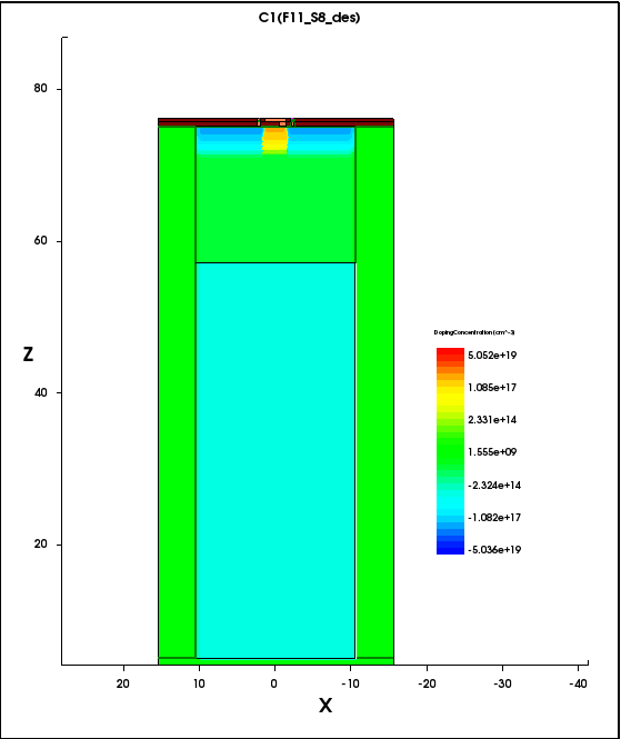
I think it’s because I have a problem with my method of using doping concentrations, because during my simulation, the carrier recombination ratio is super high, which means that my carriers are all recombination, and the following is my doping concentration distribution. ( As you can see from the graph below, their distribution is quite different)
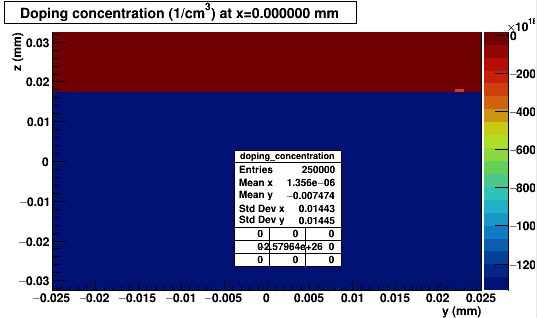
AllpixDopingTCADDoping
my cofig is:

model = “init”
dimension = 3
region = “SiEpi” “Substrate”
observable = “DopingConcentration”
xyz = x y z
divisions = 50 50 100
observable_units = “/cm/cm/cm”

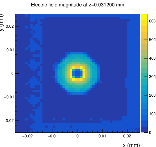
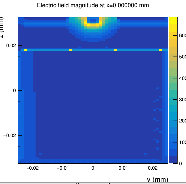
  1. I have some questions that may be more silly, for what is mentioned in the manual:

The profile is extrapolated along z such that if a position outside the sensor is queried, the last value available at the sensor surface is returned

Does this explain the content of only reporting the last Bin on the Z axis? Sorry, I don’t know if my statement is reasonable.

3.In addition, considering that the carriers are recombined during the simulation, I have read a lot of literature when doing TCAD simulations, which mentioned that some parameter values in the SRH model are not certain. Can I adjust our background script and change some of the relevant time parameters according to the relevant literature?

Hi @Isaac

  1. 30% with respect to what? Charges in the substrate will recombine and not make it to the epi. This is also true for actual MAPS sensors. If you compare your total deposited charges to the ones collected you will always get something very low. Make sure you’re correctly calculating your CCE, the measurements that have 100% also don’t take “hm, we have 50um silicon times 80eh/um so that’s 4ke”. :slight_smile:

  2. I’m sorry but I don’t understand your question. What is reported where?

  3. Currently this is not possible without changing the source code, but I took the liberty to implement this for you: Add Possibility to Define Custom Recombination Models (!986) · Merge requests · Allpix Squared / Allpix Squared · GitLab

All the best,
Simon

Dear @simonspa
Thank you for your timely reply, which is a great encouragement and help to me ~!

  1. I’m probably not being very specific. In fact, by analyzing MCTrack, I got the relevant deposited energy, and analyzed the distribution of DepositedCharge, and obtained the deposited charge distribution in the epitaxial layer region through the location position information. For the charge collection efficiency, I get it by dividing the collected charge carriers by the carriers in the epitaxial layer region. However, the efficiency is disappointing to me. Now I am analyzing module by module, so I hope to get your advice on doping concentration.

  2. You can find this information in Section 8.11 DopingConcentrationReader of the user’s manual.

  3. As for custom carrier recombination model you pointed out, I will study it carefully next. By the way, my DopingConcentration isn’t wrong? (Please excuse my possibly silly question :joy:)

Please allow me to express my sincere gratitude again for your reply

Best regards,
Isaac

Hi @Isaac

I meant:

I’m still not sure what value you mean and where it is reported. The statement from the user manual is correct - if the last step of the charge carrier goes outside the sensor, the last-seen doping concentration will be used. Otherwise you would have interesting effects at the surface. :slight_smile:

I cannot judge whether your doping profiles are correct or not. What I can tell you is that your epi layer needs to be on the topside of the sensor, i.e. at positive z. The right plot has the implant at the bottom which will not work in APSQ.

Cheers,
Simon

Hi~ @simonspa
I’m sorry to bother you again, but I couldn’t find the reason for the low charge collection efficiency myself. I think I am so stupid!
As for your previous suggestion, I think my picture may have caused some misunderstanding for you. In TCAD, its electric field, doping concentration and other distributions can be reversed for better observation. In fact, my implant is distributed in the positive Z-axis. In addition, according to your suggestion, I drew the log distribution of doping concentration, so as to see the distribution of implants.


And let me draw my electric field distribution, as shown here.

I don’t see anything wrong with it. In fact, my simulation is going to use a 5 by 5 by 5 implant as a collector to collect the electrons that are produced. My geometry and model configuration is as follows.
geometry.conf (295 Bytes)
model.conf (338 Bytes)
By analyzing the position information of deposited charge, the charge distribution of epitaxial layer is obtained. Compare the charge distribution of the epitaxial layer with that of the cluster collected charge, as shown in the figure below. We can see that the charge collection efficiency is particularly low.


The configuration information I simulated is shown below:
config.conf (1.3 KB)

DopingConcentration.txt (7.8 MB)
ElectricField.txt (9.0 MB)
I was going to try to find the cause of the problem by sifting through it myself, and try to read other people’s simulations on the forum to get some experience that would apply to me, but unfortunately, I still haven’t solved the problem.
Looking forward to your reply, I would appreciate it!

Best regards,
Isaac

Hi @Newyean @Isaac - any reason you’re using two different user accounts to post questions?

Sorry @simonspa, because we’re in the same group, and we’re stuck with the same problem. When my colleague and I discussed and edited the question, he mistakenly used his account to send the question, which I think is a “funny and stupid accident”. I’m sorry for the trouble I’ve caused you.

Best regards,
Isaac

Hi!
Sorry to bother you again after such a long time. In fact, when I reviewed the above question again, I was still confused about why the collection efficiency of my seed pixels was so low compared to the results obtained by TCAD simulation. I’d appreciate it if you could help me with some answers. (For collection efficiency, I calculated it by dividing the MPV of the seed pixel charge distribution by the MPV of the deposited charge of the epitaxial layer.)

Best regards!

Hello,

I’ve had a look at your configurations such as they were posted on the 3rd of May. I think you could do with using a finer granularity when using the mesh_converter (the electric field seems to only have 1 point per µm), but one of the main issues I think is that the electric field is a bit weird. It is not symmetric, which may lead to some odd effects.
In general however, I think that your configs produce a reasonable iron-55-ish spectrum (really single photons at 5.9 keV);

This is similar to what I expect from an ALPIDE-like sensor (with just 5000 events here, and only 1000 hitting). I set a threshold of 100 electrons to get rid of all the zero-hits.

As for how you calculate the collection efficiency, it might not be an accurate method. For a photon, charge tends to get deposited in a single “lump” basically, in this case of around 1640 electrons. If you’re looking at the “deposited charge per event” histogram from [DepositionGeant4], mind that this shows total number of charges, i.e. number of electrons plus number of holes.
I am not sure how you define which charge creation happens in the epitaxial layer, which may be another source of weirdness. Charge deposited in the substrate is very likely to recombine before it reaches the collection electrode.

Kind regards,
Håkan

Hi~!
I’m sorry for replying to your suggestion so late.

  1. You mentioned something strange about my electric field. Are you referring to the asymmetrical distribution of my electric field on both sides of the substrate?
    This part of the reason, I think, is because: in the TCAD simulation process, I not only simulated the epitaxial layer and the bottom, but also added the border around the pixel, as shown in the figure.


    The doping concentration between the boundary and the substrate is different, which affects the electric field distribution at the boundary. In addition, the doping concentration of the substrate is high, so the contribution of the substrate to the charge collected by the seed pixel is very limited.

  2. As for the charge collection efficiency:
    based on the analysis of an electron hole pair generated every 3.6eV, the energy of Fe55 is mostly about 5.9keV. Due to the setup of the implant, and the presence of the depletion zone in the actual process, it is reasonable to produce a peak in the seed pixels around 1600. But in addition, the seed pixels are not able to fully collect all the charges, and combined with the actual situation, there should be a peak around 500, that is, there is an MPV value. However, at present, we find that the peak appears at a position almost close to 0, which is not quite consistent with the actual situation.
    I was thinking, I can set collect_from_implant = 0, and when I turn collect_from_implant off, the result looks more like what I want. But I don’t know if that’s a reasonable setting, because our actual chip collects the charge from n-well.

Hi,

  1. This was not the oddity I was referring to, but this raises some further points. But first of all, I was referring to the asymmetry in the electric field that becomes visible when looking at the output plots of [ElectricFieldReader]

    This example is looking at output_plots_project = z near the collection electrode, but it’s also visible with other projections:

Now, a further point about the geometry you’re simulating; I don’t think it makes sense to simulate the edge of the pixel the way you do (but you know your sensor better than I do, I just wish to give my input as to what I think). It looks like you now have an epitaxial layer on the sides of your substrate, so basically trenches of low-doped silicon between the pixels. This is quite an unusual setup, but maybe I am misreading the colour scale in the plot you sent.
It might be a good idea to look at some linegraphs (activated in the propagation module), just to see that charges move the way you expect them to.

  1. I agree that we expect a peak at around 1600 for a 5.9 keV x-ray incidence. But then, the charge sharing will lead to a continuum to the left of it. Why do you expect a peak around 500? From the fluorescence peak, K-alpha of the silicon?
    While I agree that this would technically appear, this is a relatively rare process and will also be smeared a lot, especially in an ALPIDE-like sensor layout.

In your case, with a small collection electrode sensor, you certainly want to collect from the implant.

Kind regards,
Håkan

Hi~
Thanks for your suggestion!

  1. In order to avoid the influence of boundary on the electric field, I imported a 3*3 electric field distribution, and then only used the electric field distribution of the middle pixel for analysis. I get a picture like this, and the field distribution looks symmetrical and reasonable.
    Ele_33

2.In fact, this chip I simulated, we have tested it. Through the test found that the seed pixel charge collection situation as shown in the figure


, there is a collection peak at about 500 places. What I understand is that this peak is probably caused by charge sharing, as you mentioned.
But even after I adjusted the distribution of the electric field, the results I got were still very different from the measurements.
Seed

Hi,

  1. This is indeed a good idea to counter some asymmetries! It might still be helpful to increase the number of divisions when using mesh_converter to get the field a bit nicer. If you still have the low-doped regions at pixel edges here, this may be a source of oddness.
  2. Thanks for sharing the spectrum from data, it’s interesting. I think the peak at 500 appears because of charge loss at the pixel edges. Lower than 500 electrons, it will be increasingly rare that the seed pixel has such a low charge. You have continuous charge sharing as you come from 1600 electrons to around 500 electrons, and then you start getting threshold effects, possibly. Then at the very left, where it rises again, you likely get into noise.
    If you plot the seed pixel charge versus the cluster size, and also the total collected charge, it might give some further insight into what’s going on.

As for the simulation results, I feel like you see a similar effect, just displaced a bit. You can try playing with the threshold, but I think the charge sharing at pixel edges is what will have more of an effect (i.e. and electric field/doping map/mobility model effect). I would also here look at the cluster size and total collected charge, and compare that to the data. I would also include the K_beta in the simulations, which can be done e.g. by using the General Particle Source.

Kind regards,
Håkan

Hi~
Yes, I think the existence of peak pixel around 500 is mostly due to the deposition charge caused by incident particles at the edge of the pixel, resulting in the sharing of deposited charge between pixels.
When I define a implant following the expected charge collection process, and then deposit charge collection from the implant, I get the seed pixel charge distribution as shown in the previous message, which is not so consistent as my expectation. [collect_from_implant =1]
But something super weird happened. When I turned off the charge collection from the implant of seed pixels, I got a result that almost matched the distribution measured experimentally. As for the differences in details, I think they are acceptable.[collect_from_implant=0]
No_collect_implant

Also, my new electric field file(Change the file type from txt to init):
Ele_SUA0_S8F11_33_Boundary_xyz_ElectricField_EPI.txt (12.1 MB)

Hi @Isaac

sounds like your electric field is misaligned with respect to the implant you are defining.

btw which version of APSQ are you using?

/Simon

Hi~
I’m sorry for not replying to you in time. The version I used is v3.0.0.
Could you please tell me what is wrong with my definition of implant? I will be very grateful. :grinning:

Hi @Isaac

it’s hard to tell from your small images of the field, but the configured 5um x 5um x 5um implant seems to be too small to cover the full extent of your electrode. What happens with your collected charge distribution of you increase the size to 7um x 7um x 7um?

Background: When using the GenericPropagation module, the motion of the charge carriers will only stop when reaching the electrode volume. If this volume lies within the zero-field region of your TCAD electric field. the charge carriers will be propelled until they reach the zero-field region but then they will start diffusing (hangin’ aroung there) and never make it into the implant region. By selecting the implant region large enough to cover an area with field gradient, you make sure they reach the implant and are collected.

/Simon

Hi~
Thank you very much for your advice.
In fact, in my simulation of TCAD, the area of the Nwell part is about 8um^2, so in my simulation of Allpix, I did not set the size of implant to be particularly large, just 5x5x5
Your advice inspired me a lot. But when I adjusted my implant to a 7umx7umx7um size, I found that the simulation results were still quite different from the actual test results.
implant_7x7x7
Still not as good as [collect_from_implant=0]. Do you have any good suggestions for this situation?

Best regards!
Isaac

Hi @Isaac

…you simulate a 8um electrode, but then only set it to 7um size? These numbers were only me guessing your electrode size from a very low resolution plot. I had hoped that my explanation was sufficiently clear that the configured implant needs to be larger than the low-field region in TCAD (and therefore your 8um.

Also, line graphs are an excellent tool to understand what’s going on in your sensor, so I’d suggest you isolate an event that doesn’t return what you expect and generate a line graph for it.

/Simon