Dear Developers,
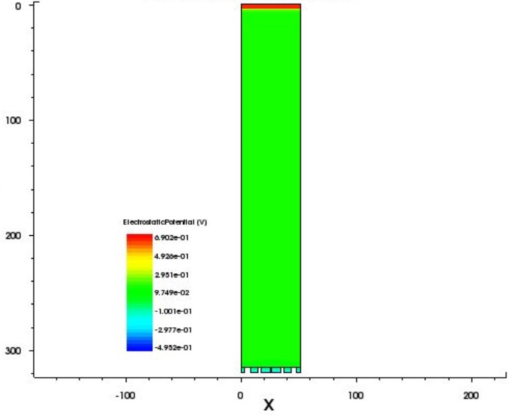
I am currently trying to use the Allpix mesh converter to convert the adaptive TCAD mesh of a FIB-milled PiN diode into a regular one. However, I cannot reproduce the same geometry with the Allpix mesh converter. Below is the electrostatic potential of the PiN diode in TCAD and the one obtained with the Allpix mesh converter.
As you can see on the top surface, there are some um-sized structures:
However, during the conversion, they get lost:
Zooming:
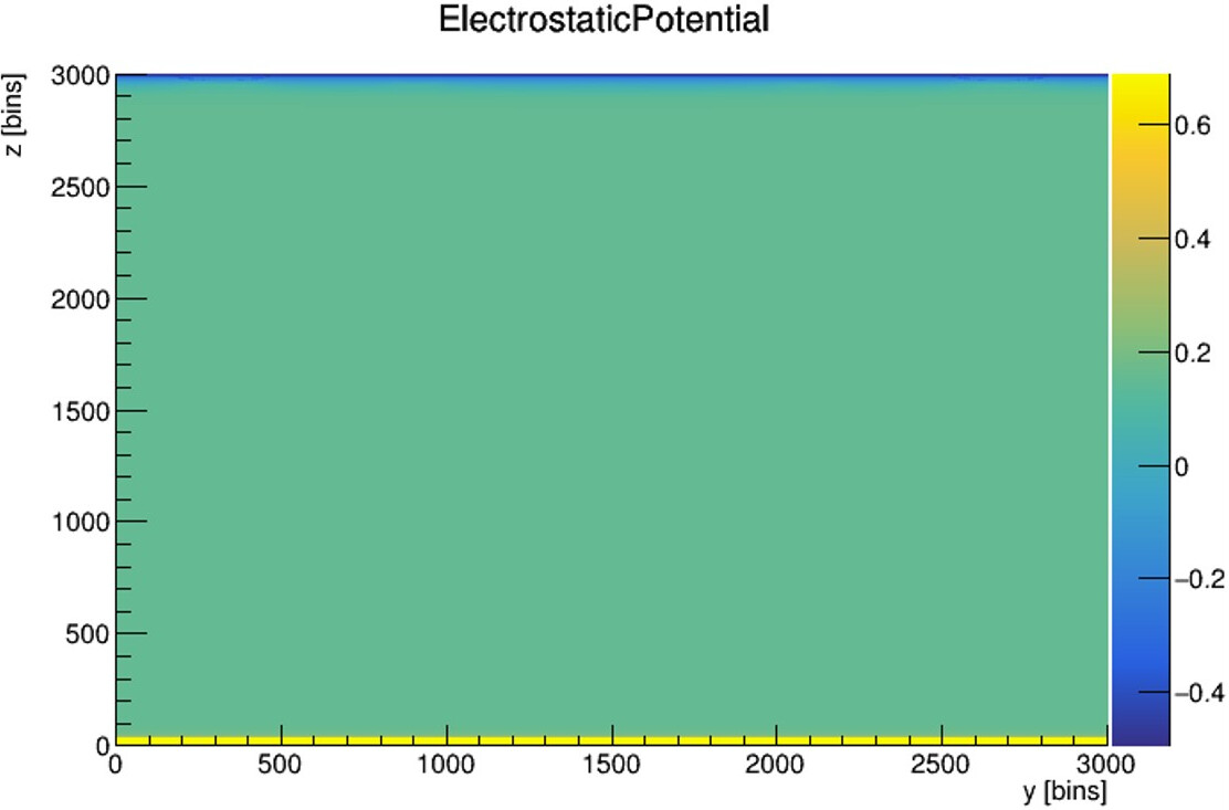
When I try to compute the weighting potential as the normalized difference between two different configurations where the bias of the electrodes (on the top of the um-sized structures) is slightly changed, I obtain the following result:
I have increased the number of divisions to 10000 (element dimension 1 x 0.0051 x 0.032 um^3) but still, obtain the same result. The adaptive mesh in TCAD is quite dense, with an intermediate step smaller than 0.5 um.
What am I missing?
Many thanks for considering my request.
Greta
1 Like
Hi @gretand
I think the converter simply interpolates between them to the nearest points it can find, which are then the ones in the “fins” (or the non-milled sections).
You could try using
allow_failure = true
to allow it to fall to zero-field values instead of increasing the search radius further and further. You of course then also need to set the radius small enough.
Does this work/
If not, we need to improve our tooling to tackle those fields! 
Simon
Hi @simonspa,
Thank you for your quick reply!
Unfortunately, I have run the simulation trying to enable the “allow_failure” option, and the result is still the same.
Kind regards,
Greta
@simonspa, correction on what I said. The max radius was not small enough. Using 8000 divisions (mesh element dimension: 1x0.006375x0.04) and a max radius of 0.6 um, this is the result:
It’s not accurate at the edge of the hollows, but the “allow failure” worked.
Greta
Hi @gretand
alright, thanks for letting me know! Maybe for the future we need to improve the converter to cover more possible configurations.
My follow-up question would now be how you treat these hollows in the subsequent simulation. One option would be to define “implants” at these positions where charge carriers would be absorbed without contributing to the signal. This is currently only available in master (or latest on CVMFS) and is documented here: Detector Models | Allpix Squared and some more info still is available on the original MR: 3D Implants, Many (!672) · Merge requests · Allpix Squared / Allpix Squared · GitLab
Cheers,
Simon