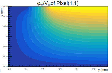
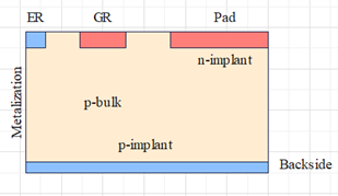
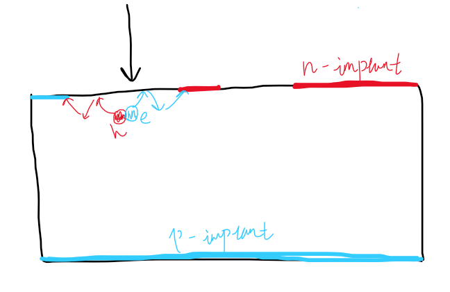
I am currently having trouble building a diode geometry (as illustrated below). My aim is to simulate the induced current on electrodes on ER,GR,Pad and Backside with a laser pulse. For testing purposes I had the WeightingPotential from the electrode on the Pad and the electric field within the diode (with the field size the same as the diode size).
My questions would be:
Is there a method to construct the geometry and define the electrodes? I have already read the Detector models in the manual but did not come up with a solution(or maybe there are other chapters about that which I did not find?). It seemed impossible to define the electrodes exactly where the implants are located within a single pixel. (Even if I divide the “diode” into pixels, it still seems hard to build this geometry.)
If we could not build this geometry, are there any alternative methods that contain the same “information” of this geometry? (I am not sure if the electric field already contains that information.) The concern is that if the electrodes are not properly defined, the charge carriers might be collected in incorrect regions, and if they suddenly stop, there would be no more induced current.
Used modules: [DepositionLaser], [Transientpropagation],[PulseTranser]
thanks for you message. To be concise, I think what you’re looking for is not yet possible in Allpix Squared. As of now, there’s no way to define custom electrodes, but only grids. Hence you would be capable of simulating the signal of the pad, but not on the other electrodes.
I fear that at the borders of the diode, indeed signals would not be generated realistically. Towards the center of the diode, this should not be much of a problem.
On the matter of what could be implemented, this sounds very tricky. Our field look-ups and signal induction calculations rely heavily on the fact that we have a regular pattern of pixels or a single electrode. Irregular patterns as the one you are showing would require a complete change in strategy, which in turn also comes with a harsh penalty in computing time. Hence I doubt that this will be implemented any time soon.
Apologies for my bad expression, I meant I would like to simulate the induced current on these 4 electrodes with their WeightingPotential respectively with 4 simulations. So for the testing I only wanted the induced current on electrode from Pad.
But I could not understand how the signal of the pad would be simulated without including the correct sensor geometry. I supposed that using only the WeightingPotential and electric field would lead to inaccurate results.(the possible reasons were mentioned above in Point 2, or maybe I misunderstood the precise function of the electrodes? )
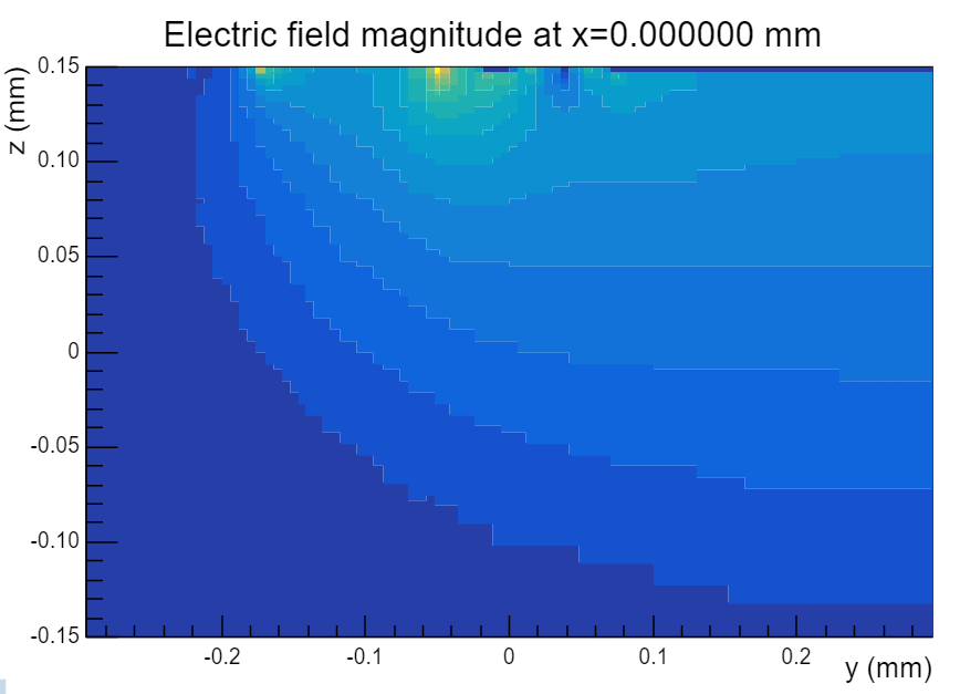
I have some testing simulations with weighting field and electric field, but the results for testing with laser positioned between GR and ER were not as expected. It seems that in our case (with 660nm at the sensor edge), the geometry we defined affected the induced current by altering the trajectories of charge carriers.
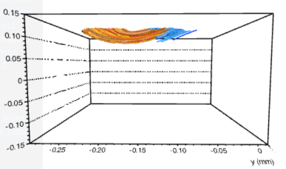
In our simulation, according to the line graph, many charge carriers simply stop their propagation at the sensor boundaries where there are no implants/electrodes defined. However, in real measurements these charge carriers would be reflected by boundaries and continue their propagation (as illustrated below).
with ER positioned(Y-axis) [10.5um, 70.5um], GR[276um,296um], Pad[366.5um,588um]
So we are now wondering if it could be possible to implement in Allpix the definition of “electrodes” areas where the charge carriers could be removed from the simulation? Everywhere on the surface where there is no electrode defined, the charge carriers should be reflected. We wanted to see how charge carriers drift near the surface between the GR and the ER.
I assume this issue (compare this post) should affect the simulations of most non-CMOS pixel and strip sensors, where the bulk is in direct contact with oxide. It should be especially prominent in simulations of strip sensors because of the large fraction of bulk-oxide interface. The geometry Peilin is using is very similar to a strip sensor where 660 nm laser light is injected between two strips.
It would be really great if it would be possible to define regions between the collecting implants where free charge carriers are not HALTED at the surface, but are reflected. For geometries where the lateral electric field (parallel to the interface) is weak there might be a large fraction of charge loss at the bulk-oxide interface. A rough modeling of charge loss at the interface could be achieved by giving the user the ability to adjust the reflection probability, so carriers which are not reflected are still HALTED (probability=0 would correspond to the current state as far as I understand).
A possible temporary workaround would be to turn off diffusion if this is possible in allpix?
alright, let’s add this effect then - should be rather straight-forward. I’d split the check for “reached sensor surface” and “reached implant/electrode”. By first checking for the latter and then for the former we can add an additional check for reflection there.
I still have to fully read Thomas’ paper, but from your summary I take that this reflection is field-dependent? How should we model this? Are there models around which describe this behavior?
I’m not aware if others have already tried to model this outside of TCAD. A realistic modeling would probably be quite difficult and computationally expensive. I didn’t mean to say the reflection probability is field-dependent (guess it is always high), but the time the carriers spend near the interface decreases with a higher lateral electric field. If the carriers spend less time in the region with a lot of defects and a low lifetime, they should be more likely to escape instead of recombining.
Setting a reflection probability would just be an effective modeling of the time carriers spend near the interface, since the longer they are there, the more likely they are to hit the interface more than once. A bit more physical modeling would probably be to set the carrier lifetime near (order of nm) the interface. I’m sure there are better ways to model this and using reflection was just one idea.
voila, let’s play a bit around with these ideas. Here is a draft MR implementing a surface_reflectivity parameter that can be set between 0.0 (no reflection) and 1.0 (total reflection). Be sure to define implants which allow the motion to be stopped!
I don’t think this will provide an adequate description of the problem, but maybe we gain some insight…