Geometric construction questions

Dear friends,

Hi, I’m a new kid about allpix2, so my question might be simple.

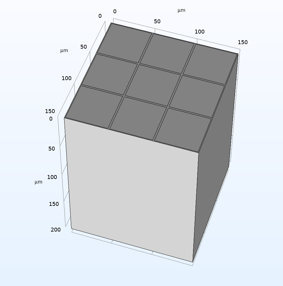
I am focusing on the geometric modeling of a simple detector which has 3×3 pixel matrix, pixel pitch is 50 um and thickness of 200 um. and my collect electrode size is 48um, so there is a 2um gap between adjacent collecting electrodes. My question is how to build this gap.

I read the documentation page about Detector Models at section 5.3, I find number_of_pixels and pixel_size to determine the base size of the sensor, but how to define the gap? Use sensor_excess?or use implant? or others?

Does the [implant] represent collect electrode? If so, why do we still need to use number_of_pixels to make division? So, my problem is that I do not knew whether these concepts (such as chip, implant, support) correspond to collect electrode. maybe because I am a beginner, so I try to find help to understand these concepts more clearly

and I already try to build a geometry construction file, don’t know if it is right. I use ‘implant’ to represent my electrodes, I first define one model, then copy this at different position, keep them attching to each other to build my 3×3 detector

#model file, name = detector_m1
type = “monolithic”
geometry = “pixel”
number_of_pixels = 1 1
pixel_size = 50um 50um
sensor_thickness = 200um
sensor_material = CADMIUM_ZINC_TELLURIDE

[implant]
type = frontside
shape = rectangle
size = 48um 48um 0.1um
#geometry file

[D1]
type = “detector_m1”
position = 0 0 0
orientation = 0 0 0

[D2]
type = “detector_m1”
position = 50um 0 0
orientation = 0 0 0

[D3]
type = “detector_m1”
position = 100um 0 0
orientation = 0 0 0

[D4]
type = “detector_m1”
position = 0um 50um 0
orientation = 0 0 0

[D5]
type = “detector_m1”
position = 50um 50um 0
orientation = 0 0 0

[D6]
type = “detector_m1”
position = 100um 50um 0
orientation = 0 0 0

[D7]
type = “detector_m1”
position = 0um 100um 0
orientation = 0 0 0

[D8]
type = “detector_m1”
position = 50um 100um 0
orientation = 0 0 0

[D9]
type = “detector_m1”
position = 100um 100um 0
orientation = 0 0 0

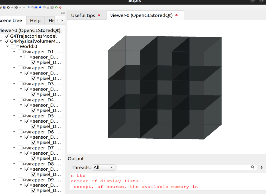
and here is a fig from [VisualizationGeant4]

Thank you in advance for your any help! May you have a happy day.
Best regards,
Solomen

To help understand my detector, I build a diagram from Comsol

Hi @solomen ,

Welcome to the forum and the framework!

There is a bit of confusion here, but I will try to straighten it out.

First of all, the way Allpix Squared works makes it easy to make pixellated detectors. It’s all built in, and this is where the keywords come in.
pixel_size sets the size of a single pixel (in the x and y directions).
number_of_pixels sets the number of pixels that make up the full sensitive region of the sensor.

The nifty thing is that Allpix Squared handles all this quite automatically. When you define a pixel by giving it an implant position and an electric field for example, this is then automatically replicated across the number of pixels you have given, also putting the pixels adjacent to each other without any barriers (allowing for charge carriers to cross pixel boundaries).

The implant is often used as the collection electrode, so in your case I would define it exactly as you have done. By default it is placed in the centre of your pixel, and in this way there will be 2 µm between adjacent collection electrodes.

What you’re currently doing is create 9 separate detectors with 1 pixel each next to each other, rather than 9 adjacent pixels of 1 detector. To amend this, set number_of_pixels = 3 3 and create just a single detector of this type in your geometry file.

In this way, each pixel will have an index within the same detector, which will be visible in hitmaps etc. An important difference to the situation you have currently is that this allows for charge sharing between pixels.

Hope this helps! Let me know if you have any further questions.

Kind regards,
Håkan

Thank you, you indeed touched on the key point.

I modified the geometry file, it looks right.

type = “monolithic”
geometry = “pixel”

number_of_pixels = 3 3
pixel_size = 50um 50um
sensor_thickness = 200um
sensor_material = MA_LEAD_IONINE

[implant]
type = frontside
shape = rectangle
size = 48um 48um 0.5um

However, there is still a small question.

I set electric field in reader module, and set collect_from_implant = true in the [SimpleTransfer] module, but the results suggest that carriers are still being collected in the gaps between pixels. Is this right?

Here are results from PropagatedCharge in my root file.

@hwennlof

If you need, here is my .conf file. Thank you again!

33.conf (1.4 KB)

Hi @solomen ,

Glad to hear it works!
I am not sure about the sensor material MA_LEAD_IONINE, but maybe you have implemented things so that this works?

Anyway, to the question; for CZT, you would get around 16300 electrons created with your source, and this will be enough with your current threshold to just about always share charge above threshold between more than one pixel if the interaction happens between two pixels.
For the propagated charge, this shows the final position of charge carriers, and this can be anywhere. “Collect from implant” just means that only charge carriers within the implant will be counted when creating a PixelHit object. Charges will still be propagated according to the electric field, and if they reach the sensor surface they will stop. With your 75 keV gammas this can likely happen anywhere in the sensor basically.
You could double-check your electric field if you haven’t by sing the output plots, making sure the mapping is as you expect it to be.
You could also look at a hitmap from the MC particle positions that cause a PixelHit if you increase the threshold. Then the pixel boundaries should be clear in that. Or an efficiency map from [DetectorHistogrammer], same effect

Kind regards,
Håkan

Thank you, buddy. Yes, I define a new material in allpix by setting fano factor and ionization_energies in source code. Maybe I should delve deeper into handling results in ROOT.

Thank you again.

1 Like