Dear allpix experts,
First excuse me for my ignorance and naivety. But I have been checking and struggling from a time without reaching a conclusion.
I am simulating CMOS MAPS sensor, ALPIDE like.
I import and convert the electric fields and the doping concentration from TCAD. (I got the TCAD files from a colleague). Here is the mesh conversion file I use:
mesh_configuration.conf (141 Bytes)
I simulate two different types of processes: the standard process called split 1, and the modified process with n-layer called split 2. These correspond to two different TCAD files.
This is the config file I am using:
main.conf (4.9 KB)
Note that the TCAD files for split 1 was produced in a different time period than the split 2 case. So I doubt that my colleague used two different methods in producing them (he is not sure but maybe he used two different TCAD versions and maybe there is an issue with the coordinate sytem and so on)
These are the simulation output files for the two cases: CERNBox
Now the issue is that I observe unexpected results for split 1, and I doubt that it is from the conversion of the TCAD files.
First, the cluster_size_map histogram for split 1 is not like it should be, on the corners it should have more yellow, as the cluster size should be four. This is the case for split2, but it should be also for split1.
Second, the cluster_size histogram shows biggder sizes for split2 compared to split1, which is unexpected, since split2 has additional n-layer that will strengthen the charge collection, which reduces charge sharing. Note that the TCAD file of split1 corresponds to 0V back bias, which should increase the sharing even more.
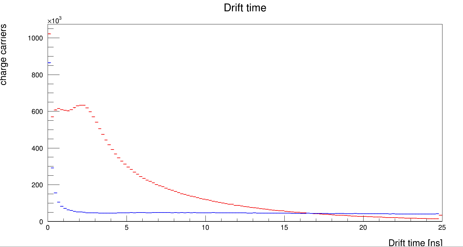
Third, I noticed also that the drift_time_histo is different between the two cases.
Any leads to what could be the problem?
Thank you and sorry for the long post, I just wanted to make things clear.
Best regards,
Hasan
Hi @hdarwish ,
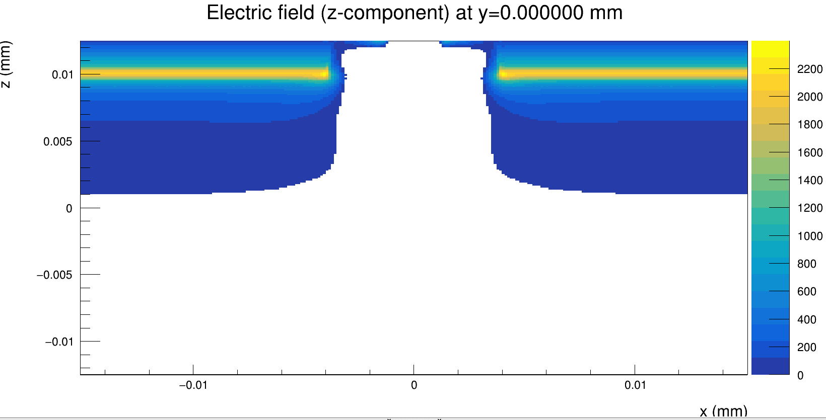
from what I can see so far, the fields look very different, as you would expect. One thing that I notice is that a large fraction of the your epi volume has a positive z component in the electric field, driving charge carriers downwards. Only the central part of the pixel shows a fully negative field. This results in a situation where charge carriers are less probable to be collected if generated anywhere but in the center of the pixel. This you can see in the cluster charge map and is also reflected in the cluster size map.
Best
Paul
1 Like
Hi @hdarwish ,
Thank you for the clear post, that always makes things easier!
The mesh conversion file looks fine, as does the main configuration. Which Allpix Squared version are you using? (Can be checked by doing allpix --version). Could you also send along your geometry configuration, and detector model? These may hold some clues, but I assume they remain identical between the two simulation runs. One thing that can be rather important is that the implant extent is correctly defined.
Now, to the detailed questions, looking at your resulting ROOT files;
- For the cluster size, it is also important to look at the efficiency. For the one you label split1, we can see that the efficiency is very low in the corners, which makes sense as it is furthest from the collection electrode and in a region with a very low electric field. This is also the region where you would get a high cluster size, but due to the low efficiency you instead get zero a lot of the time.
You could change the range of your pixel charge histograms using the max_cluster_charge keyword in [DetectorHistogrammer] or the output_plots_scale and output_plots_bins in [DefaultDigitizer], or extract and plot it using a separate script. It might give some insight to how the Landau distribution looks in this sensor and how much of it you cut away with the current threshold.
Now, for the one you label split2, we do not have much of an in-pixel efficiency map, and I’m not sure why. It is a histogram full of entries, but they are all exactly equal to 1, which does not seem right.
- This is likely related; the cluster size for split2 does indeed seem very high.
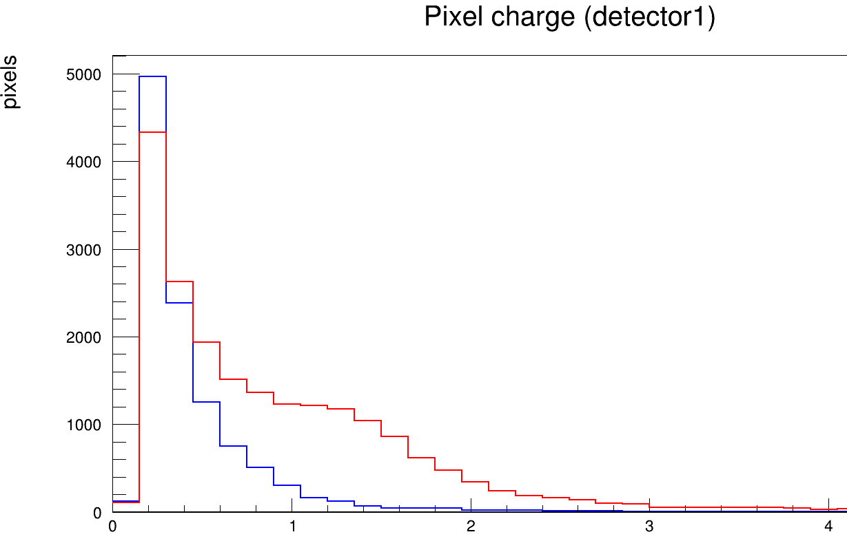
If we look at the pixel charge, there seems to be a huge difference in collected charge between the two layouts (split1 in blue, split2 in red):
This may be due to the efficiency again, but I still do not see why the efficiency is incredibly high for the split2 simulations.
- Drift time is indeed very different
So, we have faster but less complete charge collection from split1, which also indicates that we only collect charge from a relatively small region in this case.
It could be nice to make a linegraph or two, and really see how the charges move around.
The main point I would say is to check the efficiency of split2 closer, as it is too uniform and probably too high. You can try increasing the threshold to see if the expected structure appears.
I am also curious about the Allpix Squared version and the implant size used.
I really don’t see anything obviously wonky so far, it’s an interesting problem. There’s a relatively large fraction of the split1 electric field that goes in the positive z-direction, which will push charge carriers away from the collection electrode, which may explain the low efficiency here.
What’s the bias voltage for split2?
Kind regards,
Håkan
Hi @hdarwish ,
Thank you for the info, I can’t see anything very strange in the geometry. I would probably do a sensor_thickness of 50um and not have a chip_thickness at all, instead (and then being careful to set field_depth and doping_depth in the filed loaders to match the TCAD field instead).
-
I expect low efficiency in the corners for the standard layout with this kind of pixel size for the sensors used in the Tangerine project, but they have a very thin epitaxial layer. So we certainly do not get ~100% efficient there with a large pixel and a bias voltage of 0 V. For your sensors which have a thicker epitaxial layer I do not have that much intuition I’m afraid. I’m not sure which presentation you’re referring to, but due to the different epitaxial layer thicknesses, the efficiencies will not be directly comparable.
The max_cluster_charge parameter is just used to control how the cluster charge histograms look, so this suggestion was just made in order to get more sensible plots to look at. It doesn’t affect the data at all. It is more flexible to use a ROOT analysis script on the output file of [ROOTObjectWriter] instead of the [DetectorHistogrammer] however, so I’d do that instead.
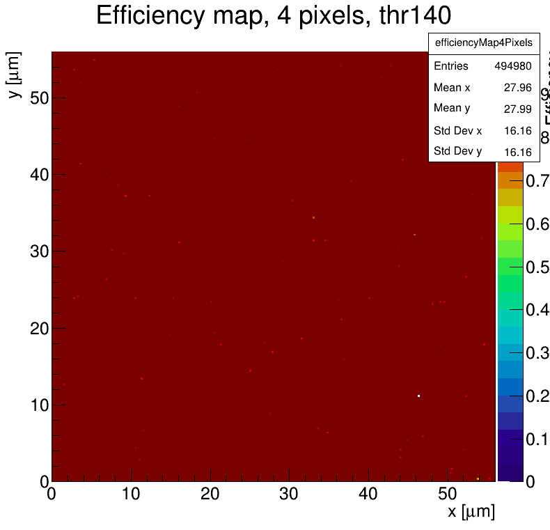
For split2, the efficiency is just too uniform. It looks like the histogram is wrong. I always get some fluctuations, and this is what I expect from a high-statistics simulation. Here’s an example form a simulation of a sensor similar to yours;
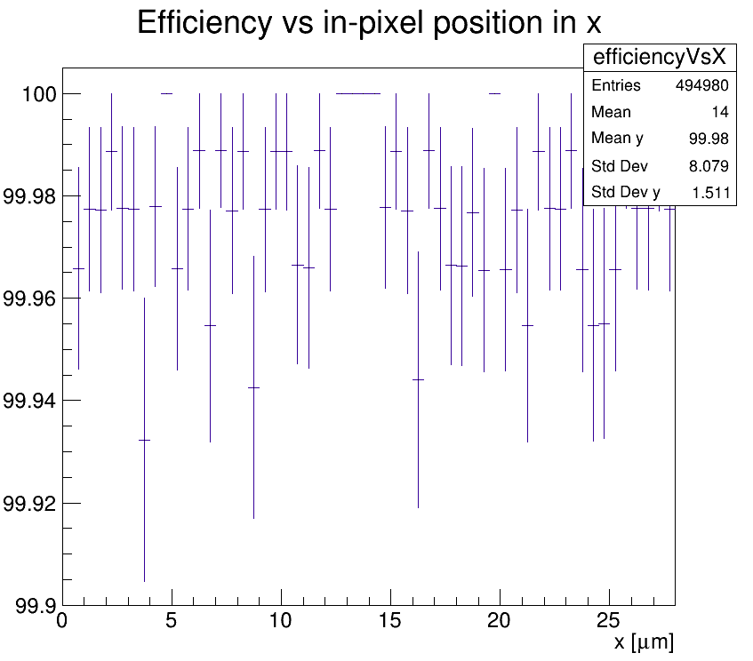
This shows the efficiency of 4 adjacent pixels, and while the efficiency is pretty uniformly equal to 1, it is not exactly 1 everywhere. Same if you look at the efficiency vs in-pixel position;
It’s basically 100% within errors everywhere, but there are errors and fluctuations.
My comment about the split2 efficiency being “too high” is likely erroneous, however, even if it should have some more fluctuations.
-
This is a bit hard to draw conclusions from, but it looks like quite a small fraction actually end up being pulled into the collection electrode. This is not unexpected at 0 V though. I am not sure what to make of this.
A big thing is probably the unexpectedly large positive E-field in your split1. Setting the minimum in the 2D plot to 0, we can just look at the positive component (pushing electrons towards negative z):
If you have the opportunity, it might be good to ask your colleague to take a closer look that everything is as it should be in the TCAD.
Kind regards,
Håkan