Dear experts,
I am simulating a CMOS MAPS sensor with standard process to estimate the charge collection efficiency for the cases of depositing charge carriers with DepositionPointCharge module.
I simulated first without recombination, and got unexpected results (CCE for the case of charge deposited near the substrate is higher than the case of depositing near the p-well)
So I decided to use the DopingConcentrationReader module to add recombination effects.
The problem is that I don’t know from where I am supposed to import this information.
I took the information of the electric field for the ElectricFieldReader module from TCAD from a colleague, but for the DopingConcentrationReader I don’t know if I should choose constant, region or mesh model and from where to get the information. (is it the same *.init I got from the mesh converter?)
Thank you for guiding me and best regards,
Hasan
Hi @hdarwish
there are several options you could implement:
- The easiest approach - and very likely sufficient to see differences already - is the
regions model. Since you mention “substrate” I am presuming you are working with a detector that implements the sensor in a high-resistivity layer, likely epitaxially grown, on top of a low-resistivity substrate wafer. In this case you’d have to separate those two, assigning the doping concentration to the two regions.
- Alternatively, your colleague that provided you with the TCAD field could provide you with a map of their simulation. In that case, they need to export the effective doping concentration instead of the electric field from TCAD - if you got e.g. DF-ISE files, likely it’s already contained.
Best,
Simon
Dear @simonspa
Thanks a lot for your reply!
When you said DF-ISE files, shouldn’t it be APF or INIT format as the manual say in the description of the DopingConcentrationReader module?
Regards,
Hasan
Hi @hdarwish
INIT or APF files always only contain a single field. Someone has converted them from the TCAD format to INIT or APF, so this needs to be done for this new observable as well.
I would recommend going with the regions approach as a first step.
Best,
Simon
@simonspa Can you please tell me how to transfer the information of the doping profile into allpix.
I read the relevant information in the manual, and I read the related topics on this forum without succeeding
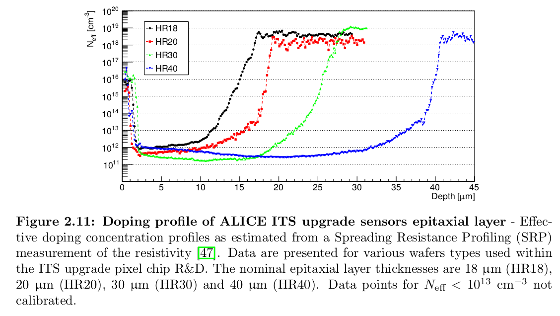
If we have a standard ALPIDE like 50um thick CMOS MAPS sensor of: substrate, 25 um epitaxial layer and p-well.
The doping profile can be seen in:
Thank you and best regards,
Very much appreciated!
Hasan
After finding a way to do this in the history here on the forum (I didn’t know before that DopingConcentrationReader is called also DopingProfileReader), I did it like this:
[DopingProfileReader]
        model = "regions"
        doping_concentration = [[2.um, 1.0e15], [20.um, 1.0e12], [25.um, 5.0e18]]
However I am not sure if it is correct. My doubt concerns the p-well and the collection diode. If we choose 2um thickness for p-well starting from the sensor surface to be 1e15 concentration, this will also include the collection diode and make it p-doped with 1e15, which doesn’t make sense at all. Since we chose only in z-axis, so we include all x and y points with thickness < 2um, including the diode, or am I wrong?
Thank you and best regards,
Hasan
Hi @hdarwish
you are using the module correctly, but I cannot help you with your simulation - only with using the software.
Best,
Simon
@simonspa Thank you!
I was asking on how the software interpret the input, if it accounts the first doping concentration to the diode also (which is not helpful) or if it exclude the diode even though it is in the first 2um thickness.
I have doubts that using the “region” parameter may have an unwanted side effect.
Thanks and best regards,
Hasan