Dear Allpix experts,
We are trying to simulate the response of an Alpide chip to charged particles using a custom TCAD electric field.
We converted the single pixel TCAD field using mesh_converter with the following config:
model = "init"
dimension = 3
region =  "substrate"
observable = "ElectricField"
observable_units = "V/mm"
divisions = 100 100 400
xyz = x y z
We used this mesh as an input to ‘all_pix’ via the ElectricFieldReader module, as follows:
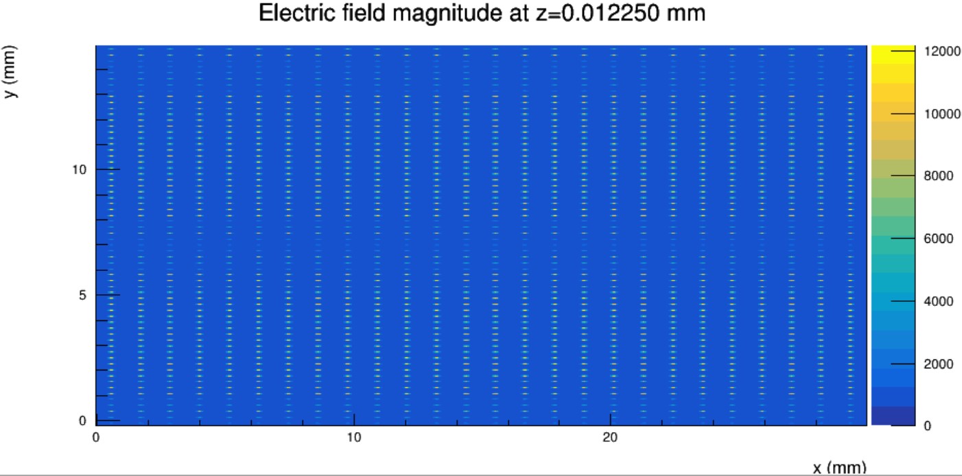
It looks like that the field read by all_pix is not correctly replicated over all the pixels in the chip. As you can see, we have fewer spots on the map respect to what we expect, i.e. 1024 x 512 pixels.
Trying to solve this behaviour, we ended up with two major doubts:
Is the replication of the field all over the pixels an automated process or should we have to specify the grid size to replicate the field?
Since at first sight our problem can be related to spatial unit of measure, where do we have to specify them in our config files both in the mesh_converter and all_pix simulator?
from the configuration you are showing all should be fine. The field scale is taken as the size of the field you are loading, the pixel size comes from your detector model file. The replication works automatically using these two parameters.
I am suspecting a binning issue in your output plot is eating the missing electrodes, this is likely also where the “pulsing” along y comes from.
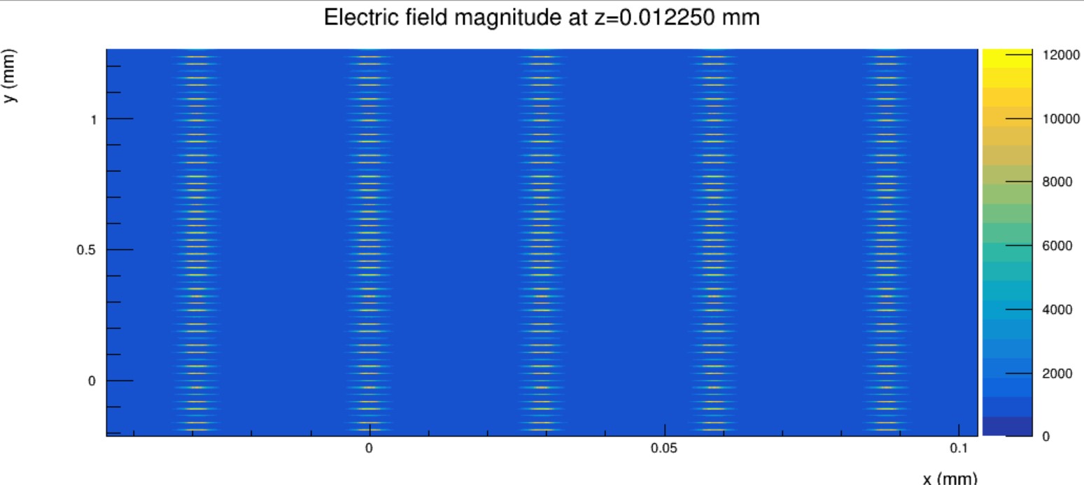
Easy way to check things: alter the detector model you are loading to only have 3x3 pixels or similar and check the alignment and replication there.
Dear @simonspa,
Thank you for your fast reply.
We performed the test you suggested by changing the alpide.conf contained in /usr/local/share/Allpix/models/ as follows:
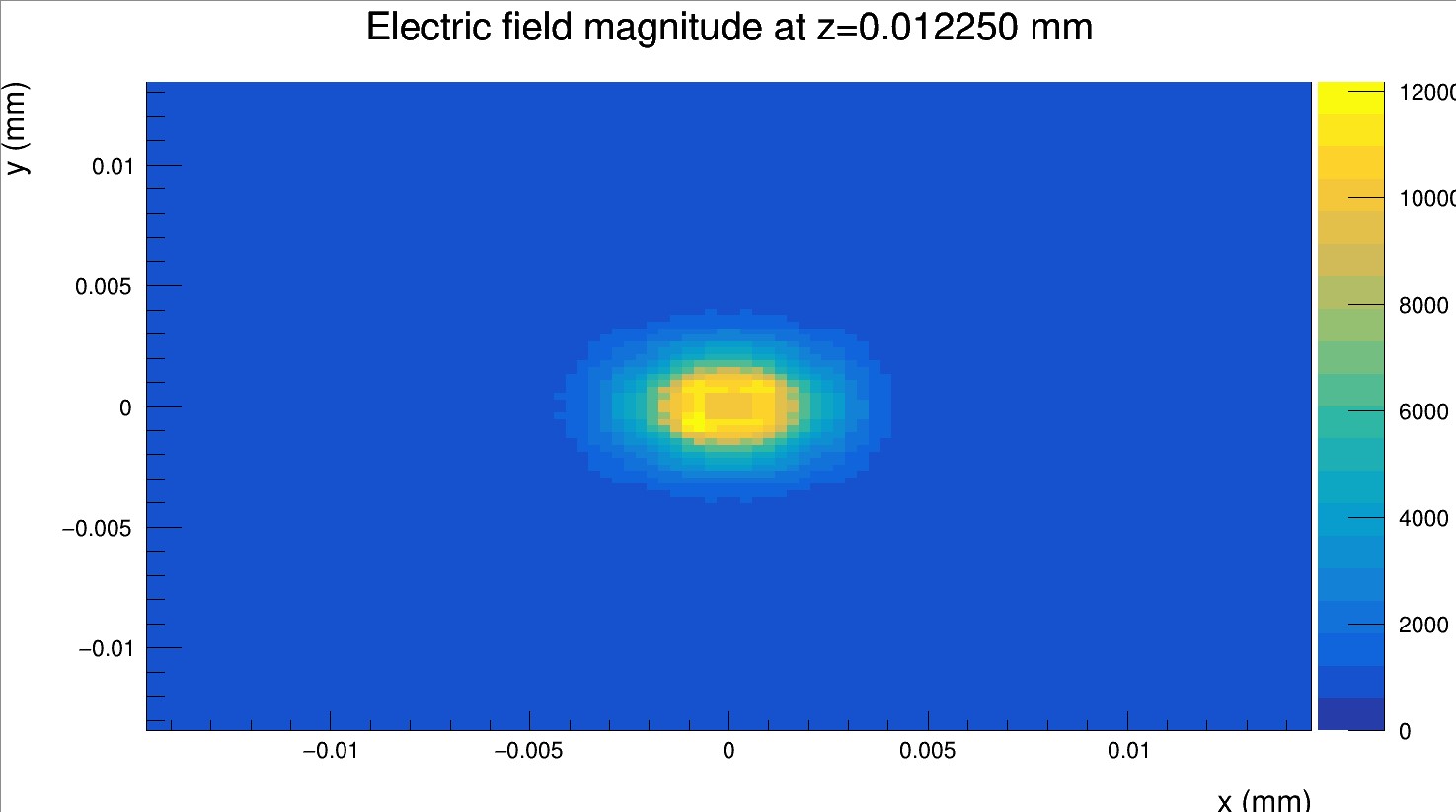
okay, probably we need to go one step back. How does your field look like when setting output_plots_single_pixel = true? If that doesn’t represent your pixel properly, then there is some issue in the field conversion.
As for your first question, the user manual has your back:
Local coordinate systems for the detectors are also right-handed Cartesian systems, with the x- and y-axes defining the sensor plane. The origin of this coordinate system is the center of the lower left pixel in the grid, i.e. the pixel with indices (0,0). This simplifies calculations in the local coordinate system as all positions can either be stated in absolute numbers or in fractions of the pixel pitch.
I.e. coordinate origin is in the pixel center, hence the lower left corner of pixel (0,0) has negative coordinates.
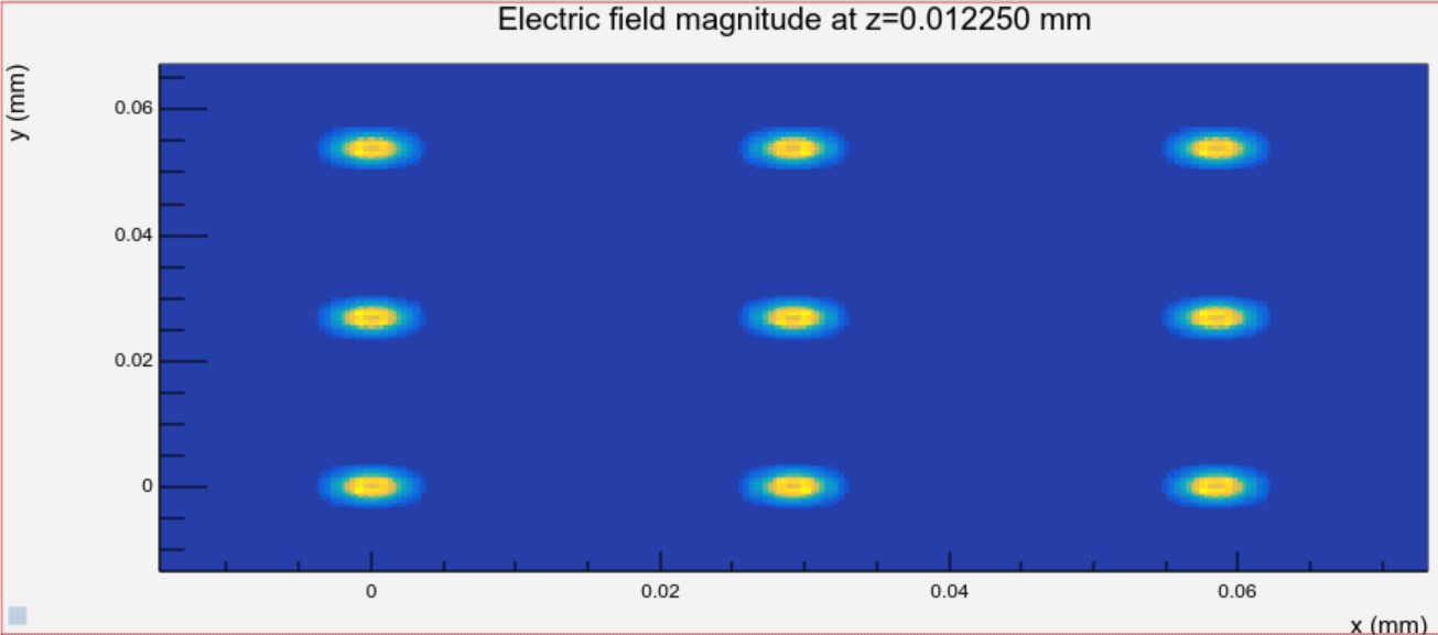
we noticed the following: your sensor has a certain sensor_excess in all directions. Look e.g. at your 3x3 plot, the absolute axes are much larger than just a 3x3 Alpide array. On your ROOT canvas, you could zoom in to the actual location of the 3x3 array (roughly -0.015 < x/y < 0.075) and you’d probably end up with the correct 3x3 array - can you confirm that?
The rest you can see in the plot is that the field is replicated throughout the sensor excess. This is something we fixed for the latest master (not yet in a release), but anyway it should not impact your simulation really, as it’s not a sensitive volume. You can of course update to the latest master, or the latest tag if you are working on CVMFS.
sorry for the confusion and thanks for sticking with us until we figured this one out. The replication of the field into the sensor excess does not have any implications on the physics since charge carriers there are ignored.
In the current master, as @pschutze mentioned, the field loading is completely reworked to provide more flexibility, and there this has already been taken care of.
Can you please tell me why did you choose the parameter region = “substrate”?
In the manual it says that it corresponds to the region name to be meshed, but I didn’t understand why the substrate should be meshed and not the epi for example which makes more sense as we are interested in the electric field in the epi.
I am simulating an alpide similar geometry chip and so I guess I will have to use the same parameters here at least.
I cannot answer for @adiluca but I can further elucidate the topic maybe. The regions to be meshed should comprise the full block of Silicon from TCAD, but exclude e.g. SiO2 surfaces or metal stacks potentially simulated. If you have chopped your silicon wafer into separate regions for epi and substrate, just add them both to the list of regions.