I am trying to convert 2D ElectricField/WeightingPotential Maps using mesh_converter, and the command I used is as below:
model = init
paser = “DF-ISE”
dimension = 2
region = N1 P1 P2 substrate
divisions = 110 110
observable = “ElectricField”
observable_units = “V/cm”
xy = xy
Similar configuration goes for the conversion of the WeightingPotential Map. However, the simulation was not able to be executed and gave the following warnings/errors
My questions are:
1): When converting 2D maps, the interpolation will happen over the yz plane, is it necessary to set the simulation in the yz plane in TCAD when running 2D simulations? If not, how should I change the .conf file?
2): Is it mandatory to use a 3D WeightingPotential map for the simulation, because the error says that the weighting potential requires a three-dimensional scalar field.
3): Should I also use 3D ElectricField Maps? But it seems like that the conversion is really time-consuming.
Sorry for the long and rather basic questions, thanks a lot in advance.
Weighting potential with 2 dimensions detected, requiring three-dimensional scalar field - this might lead to unexpected behavior.
warns you about exactly this - at least along the missing dimension, induced currents will not e physical.
If you set
ignore_field_dimensions = true
Allpix Squared will let you run the simulation anyway.
So, concering your questions:
you can swap them around using the xy parameter
See above
It really depends on your simulation if it is necessary. The conversion normally should not take long unless you selected odd starting parameters for the interpolation. If your input mesh is fine enough, you can also switch off the interpolation and just use the nearest neighbors.
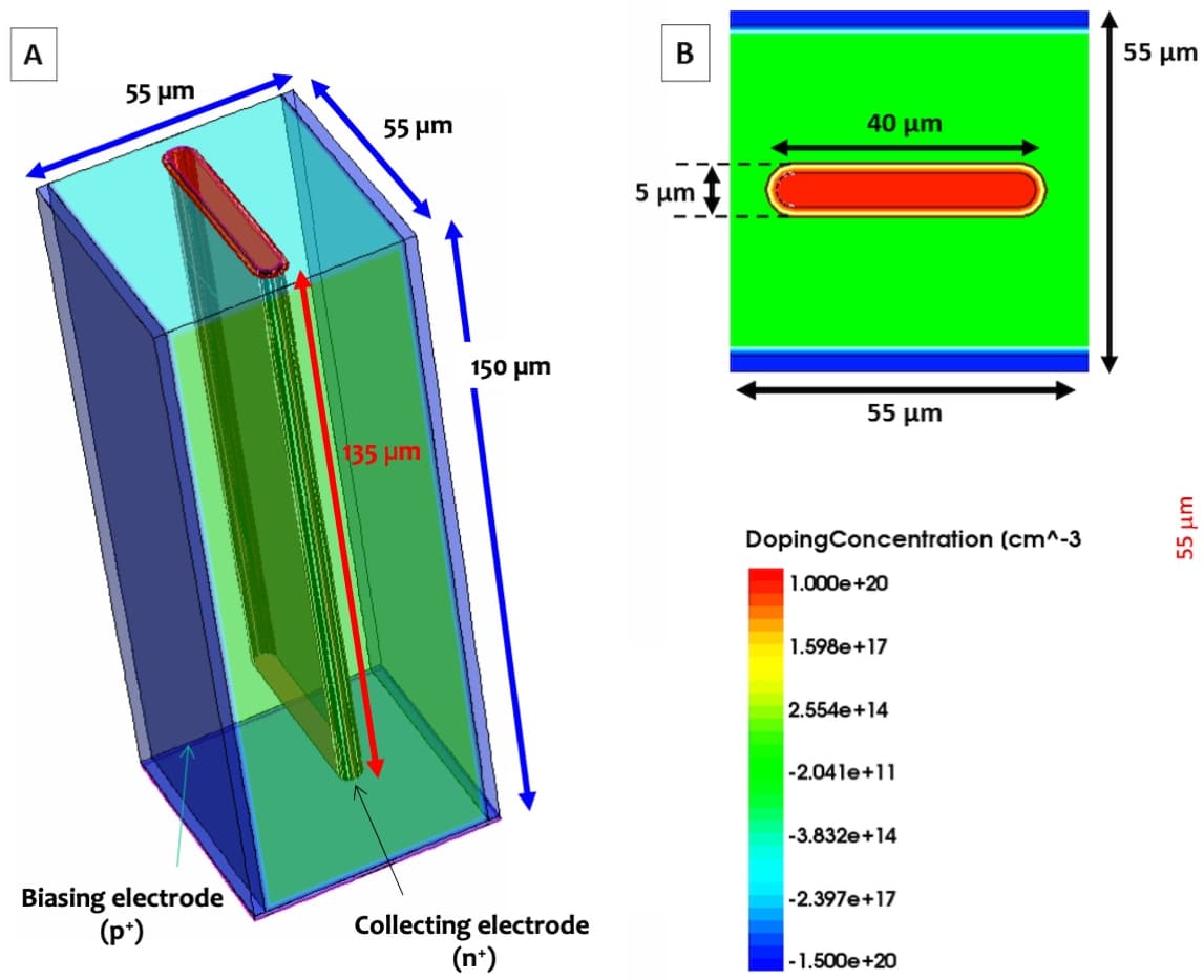
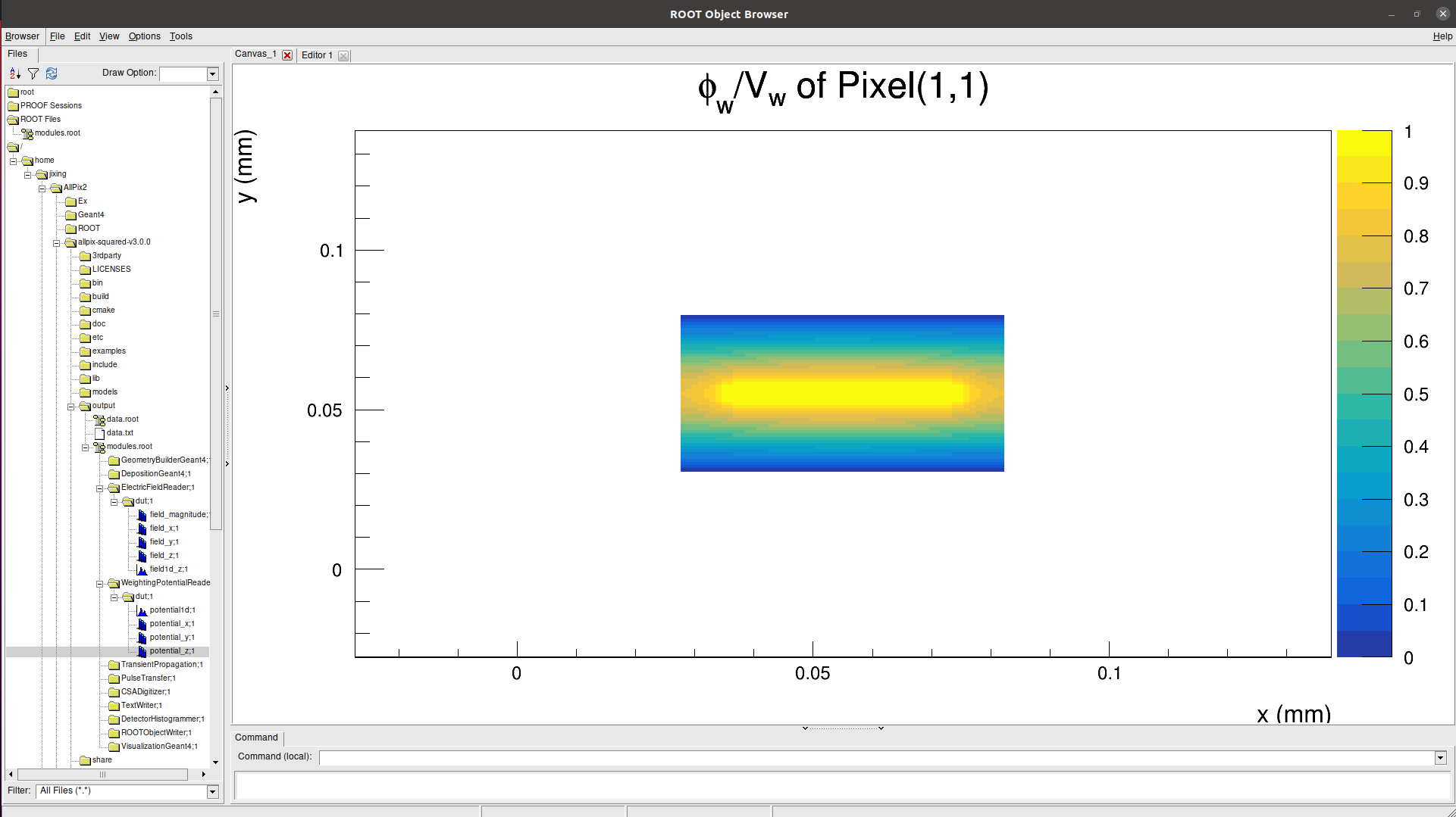
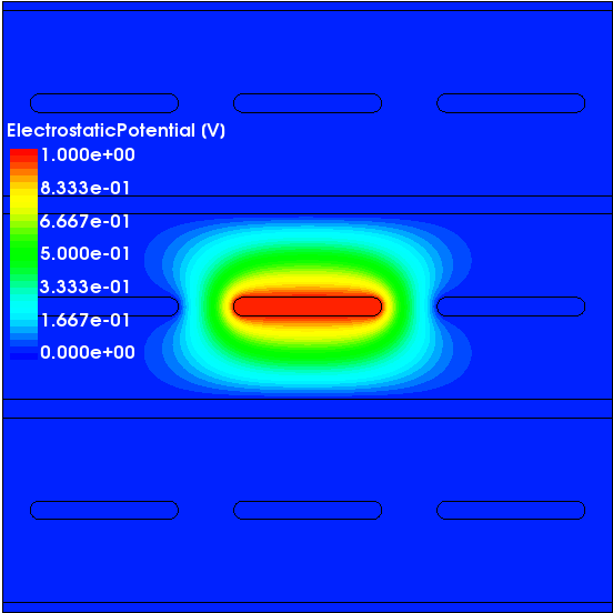
Thank you so much for the reply. Actually, I am trying to run the simulation based on detectors with 3D electrodes, see the plot below for the detailed structure.
Converted EF Map
Why this is happening is not clear to me and if I should worry about this problem. I tried to set (0, 0) to the center of the detector in TCAD and then ran the conversion again, the converted map is the same.
When converting the Weighting Potential Map, I did it based on 3D maps, however, the center of the pixel is always (55um, 55um) despite the fact that I set the center to be (0, 0) in the TCAD simulation.
Weighting Potential Map from TCAD
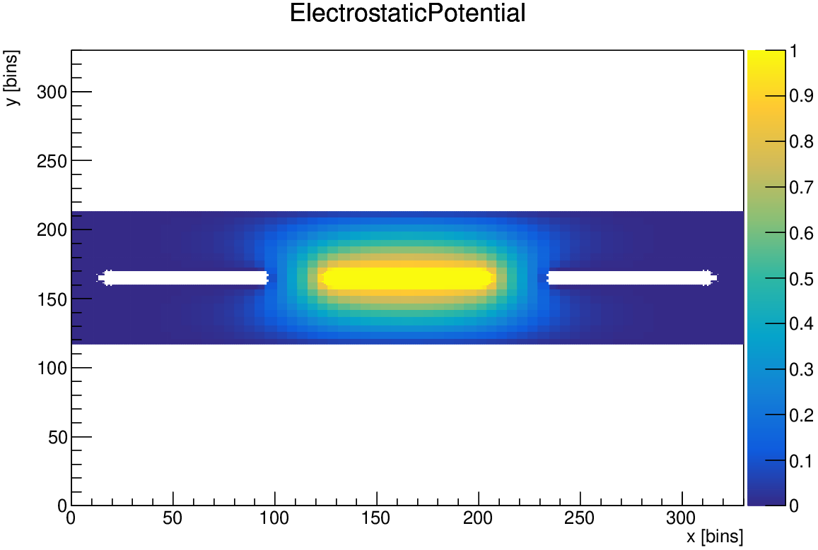
Converted Weighting Potential Map
However, this leads to a complete misalignment of the EF map and the WP map, I am not sure if it would cause any problem in the simulation since the “source_postion” and “position (of the sensor)” are mandatory parameters to be fed for the simulation?
The .conf file I used for EF conversion is as following:
model = init
paser = “DF-ISE”
region = NRect_Region P1_Region_lump_1 P1_Region_lump_2 substrate
observable = “ElectricField”
observable_units = “V/cm”
xyz = x y -z
And the .conf file I used for WP conversion is as following:
model = init
paser = “DF-ISE”
dimension = 3
region = NRect_Region P1 P2 substrate
divisions = 110 110 10
observable = “ElectrostaticPotential”
observable_units = “”
vector_field = false
xyz = x y -z
Please let me know in case there is anything unclear or anything else you need.
PS: There were people asking about the simulation of detectors with inclined 3D electrodes on the forum and your reply was negative, therefore I was wondering if it is possible to simulate 3D electrodes normal to the surface.
Thank you so much for the help in advance.
It’s actually not twice the length but three times - because your sensor is 150um deep and the pixel pitch is 55um
your orientation does not work for Allpix Squared - the z axis for us always needs to point in the direction of the sensor thickness. That means you need to flip e.g. y and z:
xyz = x z y
this is alright - what the plot shows you is the weighting potential over an area of 3x3 pixels. So the fact that the field seems to be centered at 55um,55um only tells you that it assigned it to the central pixel 1,1. If you would have a weighting potential that spans multiple pixels (which you need to get induction in neighbors - and looking at your plot with the potential being significantly larger than zero I would strongly recommend that!) you would see the central pixels along with its neighbors.
This is not a misalignment between the two fields, the lookup works entirely different. One is a “local” lookup of the field, the other one is a lookup of a field relative to an electrode position. Please have a read in the excellent section of the user manual on this:
In addition, depending on how many pixels you simulate (I hope it’s many more than just one!) the fields are automatically replicated across the whole sensor area. Please read up on the field_mapping parameter for this:
3D implants normal to the surface are possible with Allpix Squared 3.0. you need to define them in your detector model file. Also here, the manual has you covered:
Thanks a lot for the help. In response to all the suggestions:
In the TCAD simulation, I set the Z axis to point in the direction of the sensor thickness. Perhaps there is no need for me to do any kind of flipping when converting the EF/WP maps?
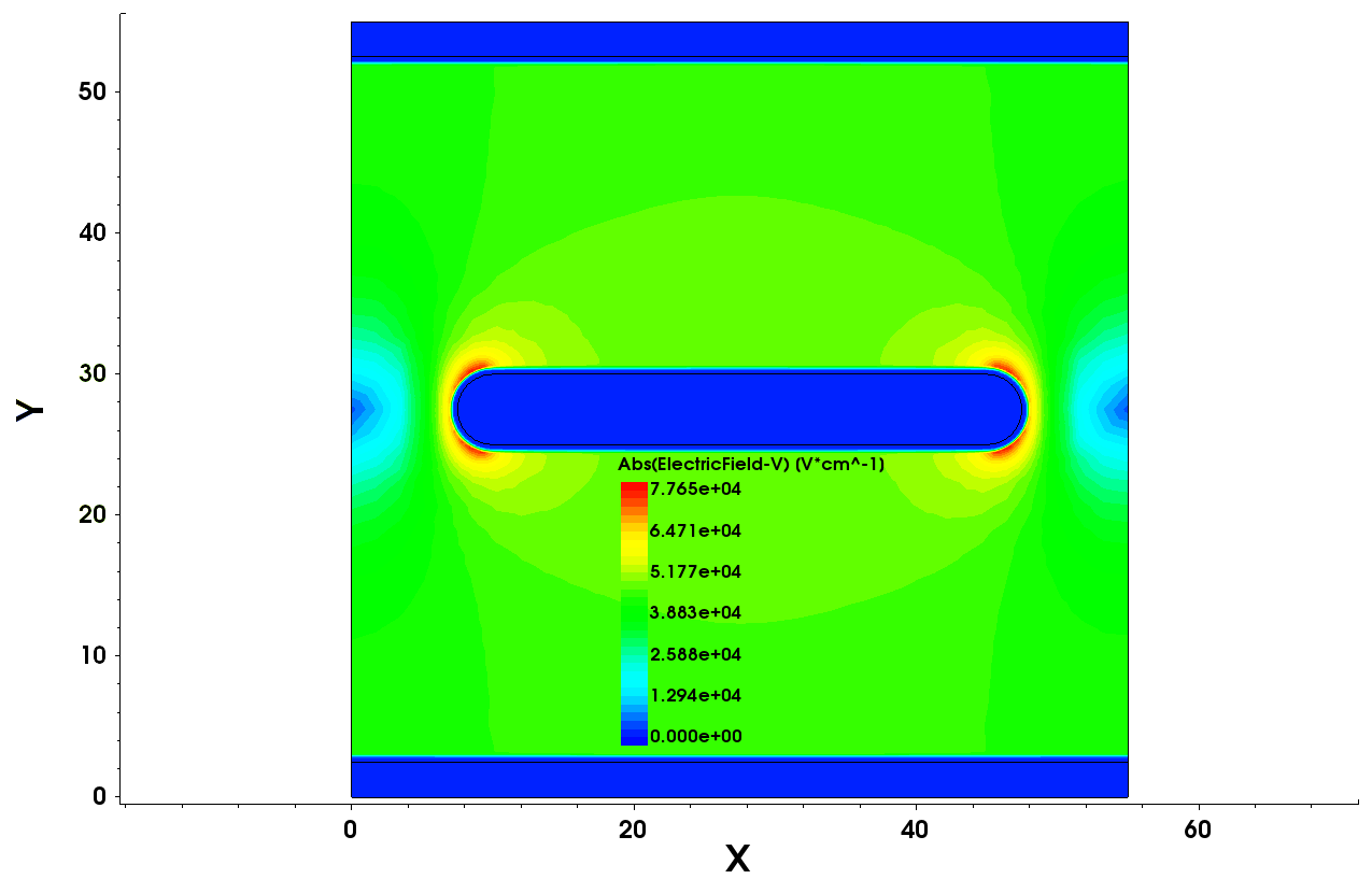
I used an area of 3*3 pixels (in 3D domain, Z corresponds to the sensor thickness) for the simulation of the weighting potential in TCAD, see the 2D cut in the following.
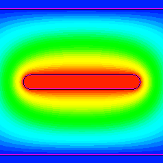
However, when I tried to plot the converted file using mesh_plotter, the two rows (of pixels) that lie outside of the central row are always blank, see the plot below.
I suppose this is normal since the blank spaces don’t contribute to the signal at all?
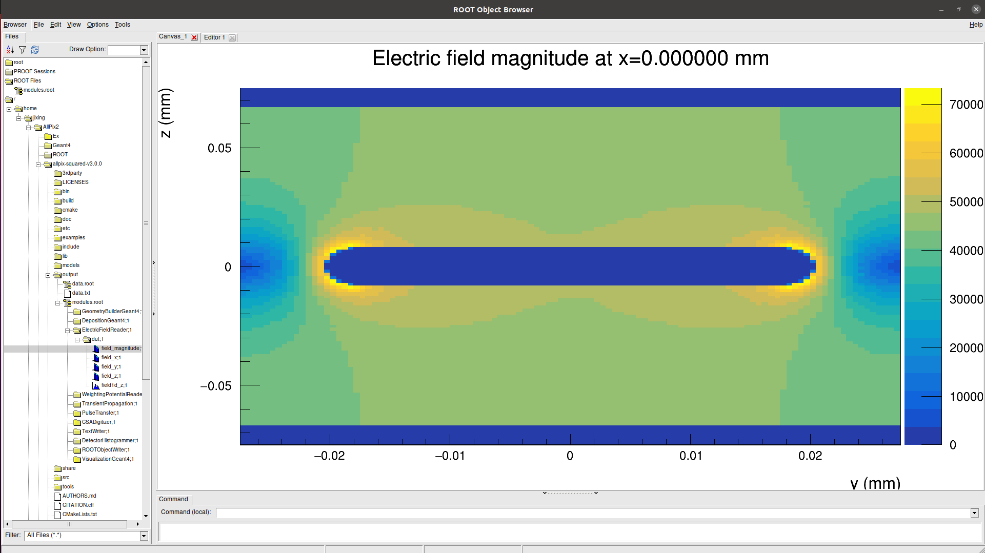
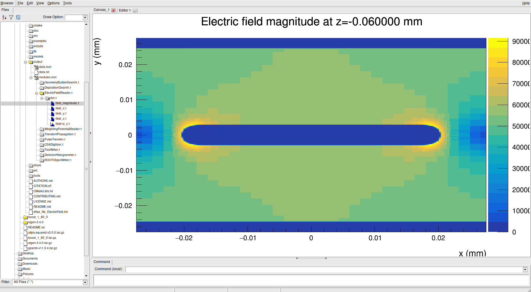
The conversion is actually very fast when I switch off the interpolation, so I used a full 3D pixel for the EF map, then I used mesh_converter to get the plots on the xy, xz, yz plane and compared them with TCAD results and they match perfectly. But I noticed that the map from [ElectricFieldReader] is actually very different from the plots I got from mesh_converter.
EF from [ElectricFieldReader]
The latter plot is not easy to interpret, and you responded to this other post saying that " the [ElectricFieldReader] does not plot your field but it plots one pixel and the field contained within". Therefore, I am not sure if I should worry about the EF map since the plots from mesh_converter look normal?
When it comes to the [implant], the “offset” defines the implant from the center of the pixel cell. This means the offset between the center of the implant and the pixel center I suppose? (Meaning that it is not the distance between the lower_left of the implant and the pixel center, or something similar).
I defined the implants in the detector model as the following, and I was wondering if there is anything wrong with them?
[implant]
size = 40um 5um 150um
orientation = 0deg
type = "frontside"
shape = "rectangle"
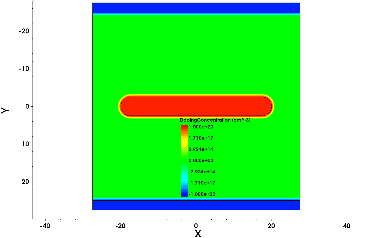
#the implant for the junction electrode, corresponds to the red region in the doping profile plot (the third plot), no offset used because the center of the implant is also the center of the pixel, the region has a total length of 40um and width 5um. PS: this region is actually rectangle+circle shaped, allpix^2 currently supports rectangle/ellipse, so I used rectangle.
[implant]
size = 55um 5um 150um
orientation = 0deg
type = "frontside"
shape = "rectangle"
offset = 0 25um
#the implant for the bottom ohmic electrode, corresponds to the bottom blue region in the doping profile plot, the region has a total length of 55um and width 5um.
[implant]
size = 55um 5um 150um
orientation = 0deg
type = "frontside"
shape = "rectangle"
offset = 0 -25um
#the implant for the top ohmic electrode, corresponds to the top blue region in the doping profile plot, the region has a total length of 55um and width 5um.
PS: Based on the converted maps, I started time-resolved simulations using [TransientPropagation] + [PulseTransfer] + [CSADigitizer], but I am not sure if there is anything wrong or inappropriate with the whole process mentioned above?
Again, thank you so much for the help.
If z is already aligned in TCAD (with the junction electrode at +z) then everything is fine already, indeed!
Hm, that’s curious. It might be that the field is absolutely zero there and hence the TH2D does show it as white? Are there any warnings printed when loading the maps?
There are several options to change which plane is plotted in the ElectricFieldReader. For a start, maybe check that the x-y plane looks the same, and then compare sensor depth for different positions of x. You can just start APSQ with -o number_of_events=0 to just do the init stage with these plots and exit.
Yes, your interpretation of offset is correct. There is one issue with your [implant] definition, and that is that all ohmic columns should be marked as backside because electrically they are not connected to the junction electrode but to the backside bias of your sensor.
Thank you so much for the help.
1). About the weighting potential map, the only warning I got when loading it in allpix^2 is “[I:WeightingPotentialReader:dut] No field units provided, interpreting field data in internal units, this might lead to unexpected results.”. I guess this is not a problem since it should be unit-less?
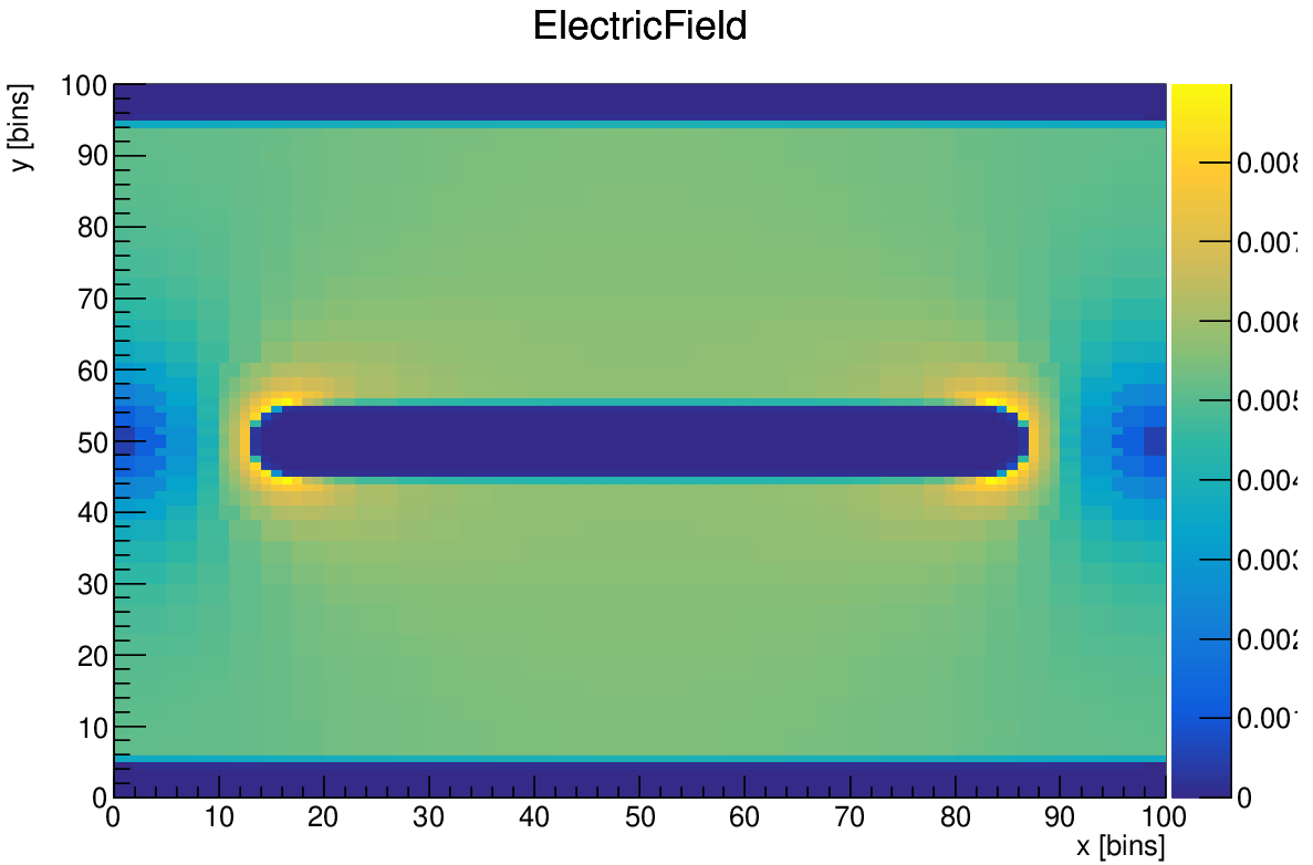
2). I tried to extract the EF map on the xy plane at different depth, and the map is normal, see the plot below.
The “field_magnitude” represents the actual projected field map, “field_x”, “field_y”, and “field_z” represents the value on the corresponding axis I suppose?
3) I changed the ohmic columns to “backside”, thanks a lot for the heads-up.
Have a nice day.
field_magnitude is \sqrt{|\vec{E}|}, the others are E_i
Since the xy plane looks reasonable, I’d switch to z-x and/or z-y and play a bit with those - just to make sure everything looks as expected also along the depth.